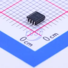
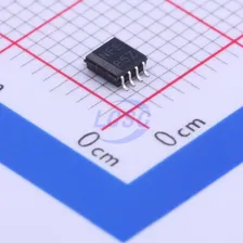
AXP1T34GMX
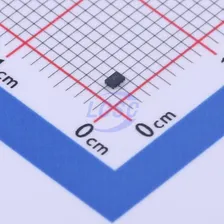
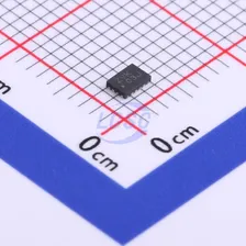
1 1 XSON-6(1x1.5) Translators, Level Shifters RoHS
Dual supply translating buffer
- Manufacturer
- Nexperia
- Manufacturer part #
- AXP1T34GMX
- Store part #
- C27438399
- Package / case
- XSON-6(1x1.5)
- Category
- Translators, Level Shifters
- Packaging
- Tape & Reel (TR)
Every Order Guarantee
100% Authentic · 30-Day Return or Replacement · policy
140 in stock
#C27438399
Stock & price checked 2 days ago
| Quantity | Unit price | Pack price |
|---|---|---|
| 1+ | ₹62.99 | ₹62.99 |
| 10+ | ₹61.47 | ₹614.70 |
| 30+ | ₹60.61 | ₹1,818.30 |
| 100+ | ₹59.52 | ₹5,952.00 |
1 × ₹62.99
₹62.99
excl. GST
₹74.33 incl. 18% GST
- Dispatch in 15-18 working days
- GST invoice with every order
- Standard pack: 5,000 per reel
AXP1T34GMX
₹62.99 for 1 + GST
Specifications
- output type
- Tri-State
- Operating Temperature
- -40℃~+125℃
- Channel Type
- Unidirectional
- Number of Elements
- 1
- Features
- Power-off protection;Output enable high-impedance
- Voltage - Supply
- 900mV~5.5V;900mV~5.5V
- Number of Circuits
- 1
Packaging & compliance
- RoHS
- ROHS3 Compliant
- Lifecycle
- Active
- ECCN
- EAR99
- Packaging
- Tape & Reel (TR)
- Standard pack
- 5,000 / Reel
- Sold per
- Piece
- Minimum order
- 1
- Unit weight
- 0.475 g
Overview
The AXP1T34 is a single bit, dual supply translating buffer. It features one input (A), an output (Y) and dual supply pins (VCCl and VCCO). Both VCCl and VCCO can be supplied at any voltage between 0.9V and 5.5V making the device suitable for translating between any voltage nodes specified (1.2V, 1.5V, 1.8V, 2.5V, 3.3V and 5.0V). No power supply sequencing is required and output glitches during power supply transitions are prevented using patented circuitry. As a result, glitches will not appear on the outputs for supply transitions during power- up/down between 20mV/μs and 5.5 V/s The input is referenced to VCCl and the output is referenced to VCCO. Schmitt- trigger action at the input makes the circuit tolerant of slower input rise and fall times. This device ensures low static and dynamic power consumption across the entire supply range and is fully specified for partial power down applications using I(OFF). The I(OFF) circuitry disables the output, preventing the potentially damaging backflow current through the device when it is powered down. In suspend mode when either VCCl or VCCO are at GND level the output is in the high- impedance OFF- state
Key features
- Wide supply voltage range:
- VCCl: 0.9 V to 5.5 V
- VCCO: 0.9 V to 5.5 V
- Low input capacitance; Ci = 1.5 pF (typical)
- Low output capacitance; CO = 3.8 pF (typical)
- Low dynamic power consumption; CPD = 0.4 pF at VCCl = 1.2 V (typical)
- Low dynamic power consumption; CPD = 11 pF at VCCO = 5 V (typical)
- Low static power consumption; ICCl = 0.1 μA (25 °C maximum)
- Low static power consumption; ICCO = 1.0 μA (25 °C maximum)
- High noise immunity
- Completes with JEDEC standard:
- JESD8-12 (1.1 V to 1.3 V; A input)
- JESD8-11 (1.4 V to 1.6 V)
- JESD8-7 (1.65 V to 1.95 V)
- JESD8-5 (2.3 V to 2.7 V)
- JESD8C (2.7 V to 3.6 V)
- JESD12-6 (4.5 V to 5.5 V)
- ESD protection:
- HBM: ANSI/ESDA/JEDEC JS-001 class 2 exceeds 2000 V
- CDM: ANSI/ESDA/JEDEC JS-002 class C3 exceeds 1000 V
- Latch-up performance exceeds 100 mA per JESD78D Class II
- Inputs accept voltages up to 5.5 V
- Low noise overshoot and undershoot < 10% of VCCO
- I(OFF) circuitry provides partial power-down mode operation
- Multiple package options
- Specified from -40°C to +125°C
Same category
More in Translators, Level Shifters
TI
SN74AVC4T774RSVR380Mbps 1 4 UQFN-16(1.8x2.6) Translators, Level Shifters RoHS
From
₹77.98
1,10,268 in stock