Avia Semicon (Xiamen)
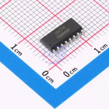
HX711SPI 2.6V~5.5V SOP-16 Analog to Digital Converters (ADC) RoHS
From
₹67.41
1,54,567 in stock
1.2V~1.8V TFBGA-121(8x8) Analog to Digital Converters (ADC) RoHS
200 Msps, 12-Bit Low-Power ADC with 8-Channel MUX
Every Order Guarantee
100% Authentic · 30-Day Return or Replacement · policy
3 in stock
#C1236523
Stock & price checked 20 h ago
| Quantity | Unit price | Pack price |
|---|---|---|
| 1+ | ₹7,278.37 | ₹7,278.37 |
| 30+ | ₹6,921.29 | ₹2,07,638.70 |
1 × ₹7,278.37
₹7,278.37
excl. GST
₹8,588.48 incl. 18% GST
MCP37211-200E/TE
₹7,278.37 for 1 + GST
The MCP37211-200 is a 12-bit 200 Msps pipelined ADC, featuring built-in high-order digital decimation filters, noise-shaping requantizer, gain and offset adjustment per channel and fractional delay recovery. The MCP37D11-200 device features digital downconversion and CW beamforming capability, in addition to the features offered by the MCP37211-200. All devices feature harmonic distortion correction and DAC noise cancellation that enable high-performance specifications with SNR of 71.3 dBFS (typical) and SFDR of 90 dBc (typical). These A/D converters exhibit low power performance with only 468 mW operation while using the LVDS interface at 200 Msps. This low-power operation coupled with high dynamic performance makes these devices ideal for various high-performance, high-speed data acquisition systems, including communications equipment, radar and portable instrumentation. In single or dual-channel mode, the Noise-Shaping Requantizer (NSR) feature can allow the ADC to improve SNR beyond a conventional 11- or 12-bit ADC. The NSR reshapes the quantization noise, such that most of the noise power is pushed outside the frequency of interest. As a result, SNR is improved significantly within a selected frequency band of interest while SFDR is not affected. The digital down-conversion option in the MCP37D10 - 200 can be utilized with the decimation and quadrature output (I and Q data) option, and offers great flexibility in various digital communication system designs, including cellular base-stations and narrow-band communication systems. The output decimation filter option improves SNR performance up to 73.7 dBFS. The digital downconversion option, in conjunction with the decimation and quadrature output options, offers great flexibility in digital communication system design, including cellular base-stations and narrow-band communications. These devices can have up to eight differential input channels through an input MUX. The sampling rate is up to 200 Msps when a single channel is used, or 25 Msps per channel when all eight input channels are used. In dual or octal-channel mode, the Fractional Delay Recovery (FDR) feature digitally corrects the difference in sampling instance between different channels, so that all inputs appear to have been sampled at the same time. AutoSync mode offers a great design flexibility when multiple devices are used in applications. It allows multiple devices to sample input synchronously at the same clock. The differential full-scale analog input range is programmable up to 2.975 Vp-P. The ADC output data can be coded in two's complement or offset binary representation, with or without the data randomizer option. The output data is available as full-rate CMOS or Double-Data-Rate (DDR) LVDS. These devices also include various features designed to maximize flexibility in the user's applications and minimize system cost, such as a programmable PLL clock, output data rate control and phase alignment and programmable digital pattern generation. The device's operational modes and feature sets are configured by setting up the user-programmable registers.
Same category
Avia Semicon (Xiamen)
HX711SPI 2.6V~5.5V SOP-16 Analog to Digital Converters (ADC) RoHS
From
₹67.41
1,54,567 in stock
MICROCHIP
MCP3421A0T-E/CHI2C 2.7V~5.5V SOT-23-6 Analog to Digital Converters (ADC) RoHS
From
₹217.09
32,994 in stock
TI
ADS1115IDGSRI2C 2V~5.5V VSSOP-10 Analog to Digital Converters (ADC) RoHS
From
₹163.15
26,705 in stock
TI
ADS1110A0IDBVRI2C 2.7V~5.5V SOT-23-6 Analog to Digital Converters (ADC) RoHS
From
₹200.98
17,231 in stock
Avia Semicon (Xiamen)
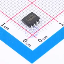
HX710A24 Bit Analog to Digital Converter 1 Input SOIC-8
From
₹48.47
16,508 in stock