
Nexperia
74LVC245APW,118Schmitt trigger 1.2V~3.6V 8 1 2.9ns@3.3V,50pF TSSOP-20 Buffers, Drivers, Receivers, Transceivers RoHS
From
₹25.94
2,31,085 in stock
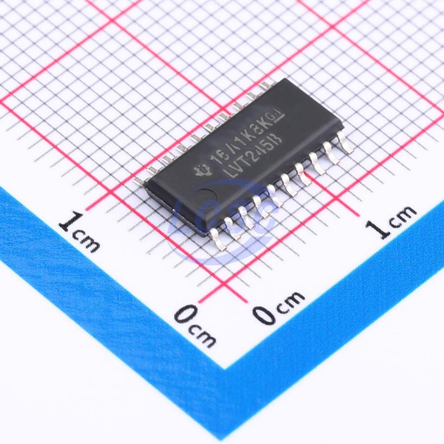
2.7V~3.6V 8 1 3.5ns@3.6V,50pF SO-20-208mil Buffers, Drivers, Receivers, Transceivers RoHS
3.3-V A-B Octal Bus Transceiver with 3-State Outputs
Every Order Guarantee
100% Authentic · 30-Day Return or Replacement · policy
16 in stock
#C2869499
Stock & price checked 3 days ago
| Quantity | Unit price | Pack price |
|---|---|---|
| 1+ | ₹114.17 | ₹114.17 |
| 10+ | ₹101.13 | ₹1,011.30 |
| 30+ | ₹88.89 | ₹2,666.70 |
| 100+ | ₹79.72 | ₹7,972.00 |
| 500+ | ₹75.85 | ₹37,925.00 |
| 1,000+ | ₹74.01 | ₹74,010.00 |
1 × ₹114.17
₹114.17
excl. GST
₹134.72 incl. 18% GST
SN74LVT245BNSR
₹114.17 for 1 + GST
This octal bus transceiver is designed specifically for low-voltage (3.3-V) VCC operation, but with the capability to provide a TTL interface to a 5-V system environment. The SN74LVT245B is designed for asynchronous communication between data buses. The device transmits data from the A bus to the B bus or from the B bus to the A bus, depending on the logic level at the direction-control (DIR) input. The output-enable (OE) input can be used to disable the device so the buses are effectively isolated. To ensure the high-impedance state during power up or power down, OE(overline) should be tied to VCC through a pullup resistor; the minimum value of the resistor is determined by the current-sinking capability of the driver. This device is fully specified for hot-insertion applications using I(off) and power-up 3-state. The I(0P) circuitry disables the outputs, preventing damaging current backflow through the device when it is powered down. The power-up 3-state circuitry places the outputs in the high-impedance state during power up and power down, which prevents driver conflict.
Similar parts — check the datasheet before substituting.
| Part | Manufacturer | Package | Stock | Price from (excl. GST) | Action | |
|---|---|---|---|---|---|---|
 | SN74LVCZ245ANSR#C1879772TI · SO-20-208mil | TI | SO-20-208mil | 10 | ₹308.29 · 10 in stock | View |
Same category
Nexperia
74LVC245APW,118Schmitt trigger 1.2V~3.6V 8 1 2.9ns@3.3V,50pF TSSOP-20 Buffers, Drivers, Receivers, Transceivers RoHS
From
₹25.94
2,31,085 in stock
TI
SN74AVC2T245RSWR1.2V~3.6V 2 2 2.4ns@3.3V,30pF WQFN-10(1.4x1.8) Buffers, Drivers, Receivers, Transceivers RoHS
From
₹41.90
1,71,155 in stock
TI
SN74LVC1G125DBVR1.65V~5.5V 1 1 3.7ns@3.3V,15pF SOT-23-5 Buffers, Drivers, Receivers, Transceivers RoHS
From
₹8.90
1,57,035 in stock
TI
SN74LV1T125DBVR1.6V~5.5V 1 1 5.5ns@5V,15pF SOT-23-5 Buffers, Drivers, Receivers, Transceivers RoHS
From
₹21.35
1,41,030 in stock
Nexperia
74HC125D,6532V~6V 1 4 11ns@4.5V,50pF SOIC-14 Buffers, Drivers, Receivers, Transceivers RoHS
From
₹18.95
1,40,760 in stock
TI
SN74LVC2G17DBVRSchmitt trigger 1.65V~5.5V 1 2 5.4ns@3.3V,50pF SOT-23-6 Buffers, Drivers, Receivers, Transceivers RoHS
From
₹24.22
1,29,655 in stock