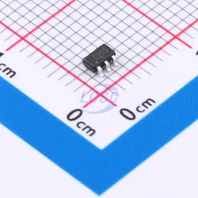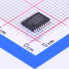
Nexperia
74LVC245APW,118Schmitt trigger 1.2V~3.6V 8 1 2.9ns@3.3V,50pF TSSOP-20 Buffers, Drivers, Receivers, Transceivers RoHS
From
₹28.71
2,48,995 in stock
2.7V~3.6V 8 1 3.1ns@3.3V,50pF SOIC-24-300mil Buffers, Drivers, Receivers, Transceivers RoHS
3.3-V AB TO OCTAL BUS TRANSCEIVERS AND REGISTERS WITH 3-STATE OUTPUTS
Every Order Guarantee
100% Authentic · 30-Day Return or Replacement · policy
19 in stock
#C1548545
Stock & price checked 24 h ago
| Quantity | Unit price | Pack price |
|---|---|---|
| 1+ | ₹431.39 | ₹431.39 |
| 10+ | ₹421.56 | ₹4,215.60 |
| 30+ | ₹414.80 | ₹12,444.00 |
| 100+ | ₹408.25 | ₹40,825.00 |
1 × ₹431.39
₹431.39
excl. GST
₹509.04 incl. 18% GST
SN74LVTH652DW
₹431.39 for 1 + GST
These bus transceivers and registers are designed for low-voltage operation at 3.3-V VCC while providing TTL interface capability to 5-V system environments. The LVTH652 device consists of bus transceiver circuits, D-type flip-flops, and control circuitry arranged to support multiplexed data transfer either directly from the data bus or from the internal storage registers. The output-enable (OEAB and OEBA) inputs control the transceiver function, and the select-control (SAB and SBA) inputs select whether real-time or stored data is transferred. The circuitry used for the select control eliminates the typical decoding glitches that occur in multiplexers during transitions between real-time and stored data. A low input selects real-time data; a high input selects stored data. Data on the A bus or B bus (or both) can be stored in the internal D-type flip-flops on the low-to-high transition of the corresponding clock (CLKAB or CLKBA) input, independent of the select-control or enable-control pins. When SAB and SBA are in the real-time transfer mode, data can be stored without using the internal D-type flip-flops by simultaneously enabling OEAB and OEBA. In this configuration, each output reinforces its input; therefore, when all other data sources on both buses are in the high-impedance state, each bus retains its last state. Active bus-hold circuitry holds unused or floating data inputs at a valid logic level. The use of pullup or pulldown resistors with the bus-hold circuitry is not recommended. When VCC is between 0 V and 1.5 V, the device is in the high-impedance state during power-up or power-down. However, to ensure the high-impedance state above 1.5 V, OE should be connected to VCC through a pullup resistor and OE should be connected to GND through a pulldown resistor; the minimum value of the resistor is determined by the current-sinking/sourcing capability of the driver. The device is fully characterized for hot-insertion applications using the Ioff and power-up three-state features. The Ioff circuit disables the outputs, preventing damaging backflow current when the device is powered down. The power-up three-state circuit places the outputs in the high-impedance state during power-up and power-down, preventing driver conflicts. The data output function can be enabled or disabled by various combinations of levels on OEAB or OEBA. The data input function is always enabled — that is, data at the bus terminals is stored on every low-to-high transition of the clock inputs. When the select control is low, the clocks can be applied simultaneously; when the select control is high, the clocks must be staggered to load both registers.
Similar parts — check the datasheet before substituting.
| Part | Manufacturer | Package | Stock | Price from (excl. GST) | Action | |
|---|---|---|---|---|---|---|
| SN74LVTH543DWR#C2675890TI · SOIC-24-300mil | TI | SOIC-24-300mil | On request | ₹274.15 · 0 in stock | View | |
Same category
Nexperia
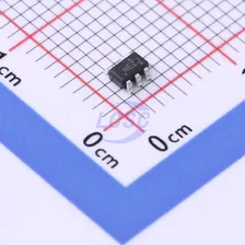
74LVC245APW,118Schmitt trigger 1.2V~3.6V 8 1 2.9ns@3.3V,50pF TSSOP-20 Buffers, Drivers, Receivers, Transceivers RoHS
From
₹28.71
2,48,995 in stock
TI
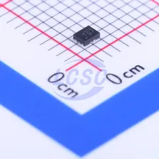
SN74LV1T125DBVR1.6V~5.5V 1 1 5.5ns@5V,15pF SOT-23-5 Buffers, Drivers, Receivers, Transceivers RoHS
From
₹21.35
2,05,900 in stock
TI
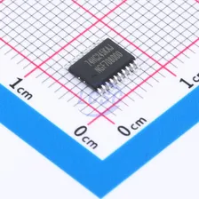
SN74AVC2T245RSWR1.2V~3.6V 2 2 2.4ns@3.3V,30pF WQFN-10(1.4x1.8) Buffers, Drivers, Receivers, Transceivers RoHS
From
₹47.40
1,63,300 in stock
TI
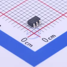
SN74LVC2G07DBVR1.65V~5.5V 1 2 3.7ns@3.3V,50pF SOT-23-6 Buffers, Drivers, Receivers, Transceivers RoHS
From
₹12.09
1,47,700 in stock