Avia Semicon (Xiamen)
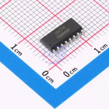
HX711SPI 2.6V~5.5V SOP-16 Analog to Digital Converters (ADC) RoHS
From
₹67.41
1,54,567 in stock

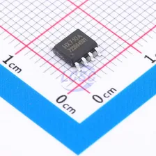
SPI 4.5V~5.5V VSSOP-8 Analog to Digital Converters (ADC) RoHS
LOW-POWER,12-BIT,SERIAL ANALOG-TO-DIGITAL CONVERTERS WITH AUTOPOWER DOWN
Every Order Guarantee
100% Authentic · 30-Day Return or Replacement · policy
3 in stock
#C2861829
Stock & price checked 7 h ago
| Quantity | Unit price | Pack price |
|---|---|---|
| 1+ | ₹5,630.60 | ₹5,630.60 |
| 10+ | ₹5,450.46 | ₹54,504.60 |
1 × ₹5,630.60
₹5,630.60
excl. GST
₹6,644.11 incl. 18% GST
TLC2552IDGK
₹5,630.60 for 1 + GST
The TLC2551, TLC2552, and TLC2555 are a family of high performance, 12-bit, low-power, miniature, CMOS analog-to-digital converters (ADC). The TLC255x family uses a 5-V supply. Devices are available with single, dual, or single pseudo-differential inputs. Each device has a chip select (CS), serial clock (SCLK), and serial data output (SDO) that provides a direct 3-wire interface to the serial port of most popular host microprocessors (SPI interface). When interfaced with a TMS320 DSP, a frame sync signal (FS) can be used to indicate the start of a serial data frame on CS for all devices or on FS for the TLC2551. The TLC2551, TLC2552, and TLC2555 are designed to operate with very low power consumption. The power saving feature is further enhanced with an autopower-down mode. This product family features a high-speed serial link to modern host processors with SCLK up to 20 MHz. The maximum SCLK frequency is dependent upon the mode of operation. The TLC255x family uses SCLK as the conversion clock, which provides synchronous operation and a minimum conversion time of 1.5 μs using a 20-MHz SCLK. The TLC2551, TLC2552, and TLC2555 are successive approximation (SAR) ADCs utilizing a charge redistribution DAC. The sampling capacitor acquires the signal on AIN during the sampling period. When the conversion process starts, the SAR control logic and charge redistribution DAC are used to add and subtract fixed amounts of charge from the sampling capacitor to bring the comparator into a balanced condition. When the comparator is balanced, the conversion is complete and the ADC output code is generated. The output data format is binary (unipolar straight binary). Zero-scale code = 000h, Vcode = GND; Full-scale code = FFFh, Vcode = VREF – 1 LSB The TLC2555 operates in pseudo-differential mode. The inverted input is available on pin 5. It can have a maximum input ripple of ±0.2 V. This is normally used for ground noise rejection. Each cycle may be started by either CS, FS, or a combination of both. The internal state machine requires one SCLK high-to-low transition to determine the state of these control signals so internal blocks can be powered up in an active cycle. Special care to SPI mode is necessary. Make sure there is at least one SCLK whenever CS (pin 1) is high to assure proper operation. Control via CS (FS = 1 at the falling edge of CS) — The falling edge of CS is the start of the cycle. The MSB may be read on the first falling SCLK edge after CS is low. Output data changes on the rising edge of SCLK. This is typically used for a microcontroller with an SPI interface, although it can also be used for a DSP. The microcontroller SPI interface may be programmed for CPOL = 0 (serial clock referenced to ground) and CPHA = 1 (data is valid on the falling edge of serial clock). At least one falling edge transition on SCLK is needed whenever CS is brought high. Control via FS — The MSB is presented after the rising edge of FS. The falling edge of FS starts the cycle. The MSB may be read on the first falling edge of SCLK after FS is low. This is the typical configuration when the ADC is the only device on the DSP serial port. Control via both CS and FS — The MSB is presented after the falling edge of CS. The falling edge of FS starts the sampling cycle. The MSB may be read on the first falling SCLK edge after FS is low. Output data changes on the rising edge of SCLK. This control via CS and FS is typically used for multiple devices connected to a TMS320 DSP. All control is provided using CS (pin 1) on the TLC2552 and TLC2555. The cycle starts on the falling edge transition provided by either a CS signal from an SPI microcontroller or FS signal from a TMS320 DSP. Timing is similar to the TLC2551, with control via CS only. The TLC2552 uses CS to reset the analog input multiplexer (MUX). A short active CS cycle (4 to 7 SCLKs) resets the MUX to AIN0. When the CS cycle time is greater than 7 SCLKs in duration, as is the case for a complete conversion cycle, (CS is low for 16 SCLKs plus maximum conversion time), the MUX toggles to the next channel. The converter sample time is 12 SCLKs in duration, beginning on the fifth SCLK received after the converter has received a high-to-low CS transition (or a high-to-low FS transition for the TLC2551). The TLC2551, TLC2552, and TLC2555 completes conversion in the following manner. The conversion starts after the 16th SCLK falling
Similar parts — check the datasheet before substituting.
| Part | Manufacturer | Package | Stock | Price from (excl. GST) | Action | |
|---|---|---|---|---|---|---|
 | ADC122S101CIMM/NOPB#C2669880TI · VSSOP-8 | TI | VSSOP-8 | 31 | ₹727.77 · 31 in stock | View |
Same category
Avia Semicon (Xiamen)
HX711SPI 2.6V~5.5V SOP-16 Analog to Digital Converters (ADC) RoHS
From
₹67.41
1,54,567 in stock
MICROCHIP
MCP3421A0T-E/CHI2C 2.7V~5.5V SOT-23-6 Analog to Digital Converters (ADC) RoHS
From
₹217.09
32,994 in stock
TI
ADS1115IDGSRI2C 2V~5.5V VSSOP-10 Analog to Digital Converters (ADC) RoHS
From
₹163.15
26,705 in stock
TI
ADS1110A0IDBVRI2C 2.7V~5.5V SOT-23-6 Analog to Digital Converters (ADC) RoHS
From
₹200.98
17,231 in stock
Avia Semicon (Xiamen)
HX710A24 Bit Analog to Digital Converter 1 Input SOIC-8
From
₹48.47
16,508 in stock