Varnitronics
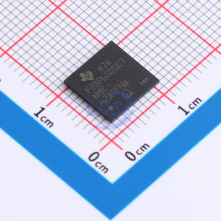
F28P650SK7NMRR TI
TI

F28P650SK7NMRR

ARM Cortex-M7 32 Bit 200MHz BGA-169 Microcontrollers RoHS

BGA-169ROHS CompliantActive
Manufacturer
TI
Manufacturer part #
F28P650SK7NMRR
Store part #
C35733946
Package / case
BGA-169
Packaging
Tape & Reel (TR)
Datasheet (PDF)

Every Order Guarantee

100% Authentic · 30-Day Return or Replacement · policy

10 in stock

#C35733946

Stock & price checked 10 days ago

QuantityUnit pricePack price
1+₹2,707.61₹2,707.61
30+₹2,597.26₹77,917.80

1 × ₹2,707.61

₹2,707.61

excl. GST

₹3,194.98 incl. 18% GST

Need volume or a scheduled delivery? Request a quote
  • Dispatch in 15-18 working days
  • GST invoice with every order
  • Standard pack: 1,000 per reel

F28P650SK7NMRR

₹2,707.61 for 1 + GST

Need this with the rest of your board? Upload the BOM — we price every line.Upload BOM

Specifications

DAC (Bit)
12bit
ADC (Bit)
16bit;12bit
Number of I/O
98
Operating Temperature
-40℃~+150℃
CPU Core
ARM Cortex-M7
Core Size
32 Bit
CPU Maximum Speed
200MHz
Oscillator Type
Built-in

Packaging & compliance

RoHS
ROHS Compliant
Lifecycle
Active
ECCN
5A992C
Packaging
Tape & Reel (TR)
Standard pack
1,000 / Reel
Sold per
Piece
Minimum order
1
Unit weight
3.92 g

Overview

TMS320F28P65x (F28P65x) is a scalable, ultra-low-latency device in the C2000 real-time microcontroller family, designed to improve the efficiency of power electronics including high power density, high switching frequency, and support for GaN and SiC technologies. Target applications include industrial motor drives (such as traction inverter motor control, HVAC motor control, mobile robot motor control), photovoltaic inverters (such as central inverters, microinverters, and string inverters), digital power supplies, HEV/EV powertrains, EV charging infrastructure, energy storage systems, industrial and collaborative robots, industrial machinery and machine tools, and industrial mobile robots. The real-time control subsystem is based on TI's 32-bit C28x DSP core, delivering 200MIPS of signal processing performance per core for floating-point or fixed-point code executed from on-chip flash or SRAM — equivalent to 400MHz processing capability on a Cortex-M7-based device. The Trigonometric Math Unit (TMU) and Vectorized CRC (VCRC) extended instruction sets further enhance C28x CPU performance, leveraging the extended instruction set for IEEE double-precision 64-bit floating-point math. The Control Law Accelerator (CLA) provides an additional 200MIPS of independent processing per core, equivalent to 280MHz processing capability on a Cortex-M7-based device. A lockstep dual-CPU comparator option along with ePIE and DMA has been added to the secondary C28x CPU for detection of permanent and transient faults. Hardware enhancements for Live Firmware Update (LFU) have been added to the F28P65x to enable fast context switching. High-performance analog blocks are tightly integrated with the processing and control units, delivering excellent real-time signal chain performance. The ADC has been enhanced with up to 40 analog channels, 22 of which feature GPIO capability, simplifying oversampling implementation; a hardware redundancy checker has been added to compare ADC conversion results across multiple ADC modules. All thirty-six frequency-independent PWMs support high resolution for controlling multiple power stages and are enhanced with Minimum Dead-Band Logic (MINDL) and Illegal Combination Logic (ICL) features. The Configurable Logic Block (CLB) allows users to add custom logic and integrate FPGA-like functionality. An EtherCAT sub-device controller and other industry-standard protocols such as CAN FD and USB 2.0 are available, while the Fast Serial Interface (FSI) enables robust communication across isolation boundaries at up to 200Mbps. The F28P65x also offers a variety of functional safety mechanisms supporting hardware encryption, secure JTAG, and secure boot.

Applications

  • Servo drive control modules (robotic servo drives), CNC control, mobile robot motor control, HVAC large commercial motor control, linear motor segmented controllers, central inverters (string inverters), power conversion systems, DC fast charging stations, inverter and motor control, industrial AC/DC, three-phase UPS, single-phase online UPS, commercial networking and server PSU, on-board chargers (OBC) and wireless chargers, automotive HVAC compressor modules, headlights

Key features

  • Real-time processing: Up to three CPUs — two 32-bit C28x DSP CPUs and one CLA CPU, all running at 200MHz; total processing capacity equivalent to a 1000MHz Arm Cortex-M7-based device for real-time signal chain performance; C28x DSP architecture includes IEEE 754 double-precision (64-bit) FPU, TMU, fast integer division (FINTDIV), CRC engine and instructions (VCRC); CLA CPU supports IEEE 754 single-precision floating point and executes code independently of the C28x CPU.
  • Memory: 1.28MB CPU-mappable flash (ECC-protected) with 5 flash banks; 248KB RAM (enhanced parity protection); EMIF supporting ASRAM, SDRAM, or ASIC/FPGA.
  • Analog subsystem: Three ADCs — 1.19MSPS each in 16-bit mode, 3.92MSPS each in 12-bit mode — up to 40 single-ended or 19 differential inputs, independent S/H per ADC, hardware post-processing of conversions with hardware oversampling (up to 128×) and undersampling modes with accumulation, averaging, and outlier rejection, 24 redundant input channels with automatic comparison of conversion results for functional safety applications; 11 window comparators with 12-bit DAC reference, DAC with slope compensation for peak and valley current mode control, internal temperature sensor and ADC reference connectivity options; two 12-bit buffered DAC outputs.
  • Control peripherals: 36 PWM channels, all with 150ps high-resolution capability (HRPWM), supporting minimum dead-band logic (MINDB), illegal combination logic (ICL), and other special functions such as diode emulation (DE), enabling matrix converters, multilevel converters, and resonant converters without additional external logic; 7 eCAP modules — 2 with HRCAP — featuring two new monitoring units for edge, pulse width, and period display, coupling with ePWM gating and trip events, 256 additional inputs for more capture options, new ADC SOC generation, and eCAP usable as additional PWM; 6 eQEP modules; 16 SDFM input channels with 2 independent filters per channel; embedded pattern generator (EPG); configurable logic block with 6 logic blocks for enhancing existing peripheral functionality or defining custom logic to reduce or eliminate external CPLD/FPGA, supporting encoder interfaces without FPGA and custom PWM generation for power conversion.
  • Communication peripherals: EtherCAT SubDevice controller (ESC); USB 2.0 (MAC + PHY); FSI supporting up to 200Mbps data exchange across isolation; 4 high-speed (up to 50MHz) SPI ports; 2 SCI (UART-capable); 2 high-speed (25Mbps) UART; two I2C interfaces (400Kbps); external boot options via SPI/SCI/I2C; 2 UART-compatible LIN modules (SCI-capable); PMBus interface (I2C-capable); 1 CAN/DCAN; 2 CAN FD/MCAN controllers with flexible data rate.
  • System peripherals: Two 6-channel DMA controllers; 185 independently programmable multiplexed GPIO pins; ePIE; LPM support; ERAD; background CRC (BGCRC).
  • Safety peripherals: AES (128/192/256) accelerator; JTAGLOCK, zero-pin boot, dual-zone security; UID; reciprocal comparison for simplified implementation; lockstep mode on C28x CPU 2; memory power-on self-test (MPOST); HWBIST on non-lockstep devices; functional safety compliant — developed for functional safety applications with documentation for ISO 26262 and IEC 61508 system design, system functionality meets ASIL D and SIL 3, hardware integrity meets ASIL B and SIL 2; ISO 26262 ASIL B certified by TÜV SÜD; IEC 61508 SIL 2 certified by TÜV SÜD.
  • Clock and system control: 2 internal 10MHz oscillators; on-chip crystal oscillator; 2 APLLs, BOR, redundant interrupt vector RAM; windowed watchdog timer module; missing clock detection circuit; dual clock comparator (DCC); live firmware update (LFU) supporting fast switching between new and old firmware in both powered-down and powered-up states; 1.2V core, 3.3V I/O design with internal VREG generating 1.2V and BOR circuit.
  • Package options: Lead-free, RoHS-compliant packages; 256-ball nFBGA [ZEJ suffix], 13mm × 13mm / 0.8mm pitch; 176-pin PowerPAD HLQFP [PTP suffix], 26mm × 26mm / 0.5mm pitch; 169-ball nFBGA [NMR suffix], 9mm × 9mm / 0.65mm pitch; 100-pin PowerPAD HTQFP [PZP suffix], 16mm × 16mm / 0.5mm pitch.
  • Temperature: Ambient temperature (T<sub>A</sub>): –40°C ~ 125°C (industrial and automotive grade qualified)

Same category

More in Microcontrollers

View all

Raspberry Pi

RP2040

ARM Cortex-M0+ 32 Bit 133MHz LQFN-56(7x7) Microcontrollers

From

₹145.12

56,634 in stock