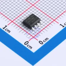
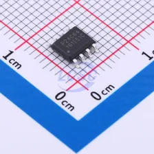
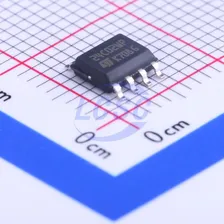
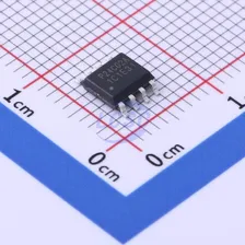
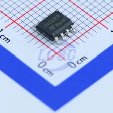
25CSM04-I/MF
4Mbit 8MHz SPI TDFN-8-EP(5x6) Memory
4-Mbit SPI Serial EEPROM with 128-Bit Serial Number and Enhanced Write Protection
Every Order Guarantee
100% Authentic · 30-Day Return or Replacement · policy
11 in stock
#C1019738
Stock & price checked 3 days ago
| Quantity | Unit price | Pack price |
|---|---|---|
| 1+ | ₹780.64 | ₹780.64 |
| 10+ | ₹763.21 | ₹7,632.10 |
| 30+ | ₹751.46 | ₹22,543.80 |
| 100+ | ₹739.93 | ₹73,993.00 |
1 × ₹780.64
₹780.64
excl. GST
₹921.16 incl. 18% GST
- Dispatch in 15-18 working days
- GST invoice with every order
- Standard pack: 98 per tube
25CSM04-I/MF
₹780.64 for 1 + GST
Specifications
- Operating Temperature
- -40℃~+85℃
- Features
- Hardware write protection function;Built-in power-on reset (POR);Built-in error correction code (ECC) function;Built-in write enable latch (WEL);Software write protection function
- Memory Size
- 4Mbit
- Voltage - Supply
- 2.5V~5.5V;3mA
- Clock Frequency
- 8MHz
- Access Time
- 40ns;80ns
- Data Retention - TDR (Year)
- 100 Years
- Write Cycle Time(tWC)
- 5ms
- Standby Supply Current
- 2uA
- Interface
- SPI
- Write Cycle Endurance
- 1,000,000 cycles
Packaging & compliance
- RoHS
- RoHS
- Lifecycle
- Active
- ECCN
- EAR99
- Packaging
- Tube-packed
- Standard pack
- 98 / Tube
- Sold per
- Piece
- Minimum order
- 1
- Unit weight
- 0.527 g
Overview
The 25CSM04 provides 4 Mbits of Serial EEPROM utilizing the Serial Peripheral Interface (SPI) compatible bus. The device is organized as 524,288 bytes of 8 bits each (512 Kbyte) and is optimized for use in consumer and industrial applications where reliable and dependable nonvolatile memory storage is essential. The 25CSM04 is capable of operation across a broad voltage range (2.5V to 5.5V). The bus signals required are a clock input (SCK) plus separate data in (SI) and data out (SO) lines. Access to the device is controlled through a Chip Select (CS) input. Communication to the device can be paused via the HOLD pin. While the device is paused, transitions on its inputs will be ignored, with the exception of Chip Select, allowing the host to service higher priority interrupts. The 25CSM04 features a nonvolatile Security register independent of the 4 Mbit main memory array. The first half of the Security register is read-only and contains a factory-programmed, globally unique 128-bit serial number in the first 16 bytes. The 128-bit serial number is unique across the entire CS series of Serial EEPROM products and eliminates the time consuming step of performing and ensuring serialization of a product on a manufacturing line. The 128-bit read-only serial number is followed by an additional 256 bytes of user-programmable EEPROM. The user-programmable section of the Security register can later be permanently write-protected via a software sequence. The 25CSM04 features a configurable write protection scheme which allows the user to select Legacy Write Protection mode or Enhanced Write Protection mode. Legacy Write Protection mode enables the Block Protection function via the STATUS register. Enhanced Write Protection mode segments the memory into independent partitions. Each partition can be configured to inhibit writing based on the status of the Memory Partition register setting. For added reliability the 25CSM04 uses a built-in Error Correction Code (ECC) scheme. This scheme can correct up to one incorrectly read bit within four bytes read out. Additionally, the 25CSM04 includes a flag in the STATUS register to report if any errors were detected and corrected in the most recent memory array read sequence. The 25CSM04 features an identification register that contains identification information that can be read from the device. This enables the application to electronically query and identify the 25CSM04 while it is in the system. The identification method and the instruction opcode comply with the JEDEC standard for “Manufacturer and Device ID Read Methodology for SPI Compatible Serial Interface Memory Devices”. The type of information that can be read from the device includes the JEDEC defined Manufacturer ID, the vendor-specific Device ID, and the vendor-specific Extended Device Information (EDI).
Key features
- 4-Mbit Serial EEPROM:
- 524,288x8 organization
- Page size of 256 bytes
- Byte or sequential reads
- Byte or page writes
- Self-timed write cycle (5 ms maximum)
- Security Register:
- Preprogrammed 128-bit serial number
- 256-byte user-programmable lockable ID page
- Built-in Error Correction Code (ECC) Logic:
- ECC Status bit via the STATUS register
- JEDEC SPI Manufacturer Read ID Support
- High-Speed Clock Frequency:
- 8 MHz at VCC ≥ 3.0V
- 5 MHz at VCC ≥ 2.5V
- Legacy Write Protection Mode:
- Block protection functionality (quarter, half or entire memory array)
- Enhanced Write Protection Mode:
- User-definable memory partitions
- Each partition can be set independently and have unique protection behavior
- Low-Power CMOS Technology:
- Voltage range: 2.5V to 5.5V
- Write current: 3.0 mA at 5.0V
- Read current: 3.0 mA at 5.0V, 8 MHz
- Standby current: 1.0 μA at 2.5V (I-Temp.)
- High Reliability:
- More than one million erase/write cycles
- Built-in ECC logic for increased reliability
- Data retention: > 100 years
- ESD protection: > 4000V
- Available Temperature Ranges:
- Industrial (I): -40℃ to +85℃
Alternatives
Similar parts — check the datasheet before substituting.
| Part | Manufacturer | Package | Stock | Price from (excl. GST) | Action | |
|---|---|---|---|---|---|---|
| 25CSM04T-I/MF#C1513066MICROCHIP · TDFN-8-EP(5x6) | MICROCHIP | TDFN-8-EP(5x6) | On request | ₹834.98 · 0 in stock | View | |
Same category