


STC Micro
STC8H1K08-36I-TSSOP2051 Series 8 Bit 33MHz TSSOP-20 Microcontrollers RoHS
From
₹42.36
1,52,934 in stock
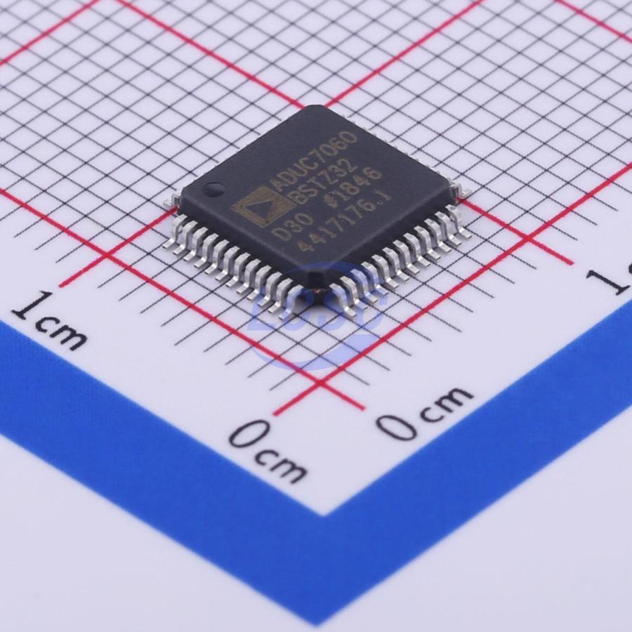
Other ARM Series 16/32 Bit 10MHz LQFP-48(7x7) Microcontrollers RoHS
Low Power, Precision Analog Microcontroller, Dual Sigma-Delta ADCs, Flash/EE, ARM7TDMI
Every Order Guarantee
100% Authentic · 30-Day Return or Replacement · policy
1 in stock
#C411336
Stock & price checked 2 days ago
| Quantity | Unit price | Pack price |
|---|---|---|
| 1+ | ₹1,556.93 | ₹1,556.93 |
| 10+ | ₹1,338.98 | ₹13,389.80 |
| 30+ | ₹1,206.01 | ₹36,180.30 |
| 100+ | ₹1,094.74 | ₹1,09,474.00 |
1 × ₹1,556.93
₹1,556.93
excl. GST
₹1,837.18 incl. 18% GST
ADUC7060BSTZ32-RL
₹1,556.93 for 1 + GST
The ADuC706x series are fully integrated, 8 kSPS, 24-bit data acquisition systems incorporating high performance multichannel sigma-delta (Σ-Δ) analog-to-digital converters (ADCs), 16-bit/ 32-bit ARM7TDMI MCU, and Flash/EE memory on a single chip. The ADCs consist of a primary ADC with two differential pairs or four single-ended channels and an auxiliary ADC with up to seven channels. The ADCs operate in single-ended or differential input mode. A single-channel buffered voltage output DAC is available on chip. The DAC output range is programmable to one of four voltage ranges. The devices operate from an on-chip oscillator and a PLL generating an internal high frequency clock up to 10.24 MHz. The microcontroller core is an ARM7TDMI, 16-bit/32-bit RISC machine offering up to 10 MIPS peak performance; 4 kB of SRAM and 32 kB of nonvolatile Flash/EE memory are provided on chip. The ARM7TDMI core views all memory and registers as a single linear array. The ADuC706x contains four timers. Timer1 is a wake-up timer with the ability to bring the part out of power saving mode. Timer2 is configurable as a watchdog timer. A 16-bit PWM with six output channels is also provided. The ADuC706x contains an advanced interrupt controller. The vectored interrupt controller (VIC) allows every interrupt to be assigned a priority level. It also supports nested interrupts to a maximum level of eight per IRQ and FIQ. When IRQ and FIQ interrupt sources are combined, a total of 16 nested interrupt levels is supported. On-chip factory firmware supports in-circuit serial download via the UART serial interface ports and nonintrusive emulation via the JTAG interface. The parts operate from 2.375 V to 2.625 V over an industrial temperature range of -40℃ to +125℃.
Similar parts — check the datasheet before substituting.
| Part | Manufacturer | Package | Stock | Price from (excl. GST) | Action | |
|---|---|---|---|---|---|---|
 | ADUC7060BSTZ32#C30066ADI · LQFP-48(7x7) | ADI | LQFP-48(7x7) | 3 | ₹1,650.50 · 3 in stock | View |
Same category
STC Micro
STC8H1K08-36I-TSSOP2051 Series 8 Bit 33MHz TSSOP-20 Microcontrollers RoHS
From
₹42.36
1,52,934 in stock
STC Micro
STC8G1K08A-36I-SOP851 Series 8 Bit 36MHz SOP-8 Microcontrollers RoHS
From
₹35.85
82,120 in stock
PUYA
PY32F002BF15U6TRARM Cortex-M0+ 32 Bit 24MHz QFN-20-EP(3x3) Microcontrollers
From
₹23.25
80,535 in stock
SILICON LABS
EFM8BB21F16G-C-QFN20R51 Series 8 Bit 50MHz QFN-20-EP(3x3) Microcontrollers RoHS
From
₹167.39
59,815 in stock




