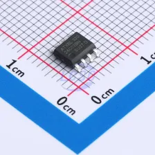
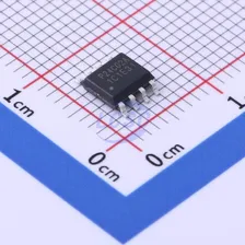
AT45DB021E-SSHNHC-T
2Mbit 1.65V~3.6V 85MHz SPI Memory RoHS
Every Order Guarantee
100% Authentic · 30-Day Return or Replacement · policy
10 in stock
#C22327876
Stock & price checked 2 days ago
| Quantity | Unit price | Pack price |
|---|---|---|
| 1+ | ₹346.64 | ₹346.64 |
| 10+ | ₹338.91 | ₹3,389.10 |
| 30+ | ₹333.77 | ₹10,013.10 |
| 100+ | ₹328.63 | ₹32,863.00 |
1 × ₹346.64
₹346.64
excl. GST
₹409.04 incl. 18% GST
- Dispatch in 15-18 working days
- GST invoice with every order
- Standard pack: 4,000 per reel
AT45DB021E-SSHNHC-T
₹346.64 for 1 + GST
Specifications
- Operating Temperature
- -40℃~+85℃
- Features
- Power-on reset;Hardware write protection;Software write protection;Absolute write protection
- Memory Size
- 2Mbit
- Voltage - Supply
- 1.65V~3.6V
- Program / Erase Cycles
- 100,000 cycles
- Clock Frequency
- 85MHz
- Data Retention - TDR (Year)
- 20 Years
- Standby Supply Current
- 25uA
- Interface
- SPI
Packaging & compliance
- RoHS
- ROHS3 Compliant
- Lifecycle
- Active
- ECCN
- EAR99
- Packaging
- Tape & Reel (TR)
- Standard pack
- 4,000 / Reel
- Sold per
- Piece
- Minimum order
- 1
- Unit weight
- 0.51 g
Overview
The AT45DB021E is a serial-interface, sequential-access Flash memory with a minimum operating voltage of 1.65V. It is well-suited for a wide range of applications including digital voice, image, program code, and data storage. The device also supports the RapidS serial interface for applications requiring high-speed operation. Its 2,162,688-bit memory is organized as 1,024 pages of either 256 bytes or 264 bytes. In addition to the main memory, the AT45DB021E includes a 256/264-byte SRAM buffer. This buffer can be used as additional system scratch memory, and EEPROM emulation (bit or byte alterability) is easily achieved through self-contained, three-step read-modify-write operations. Unlike conventional Flash memories that use multiple address lines and a parallel interface for random access, this device accesses its data sequentially using a serial interface. This simple sequential access significantly reduces the effective pin count, simplifies hardware layout, improves system reliability, and minimizes switching noise.
Applications
- Digital voice storage
- Image storage
- Program code storage
- Data storage
Key features
- Single supply voltage: 1.65V to 3.6V
- SPI-compatible, supports SPI Modes 0 and 3, RapidS operation
- Continuous read capability across the entire array
- Up to 85MHz operation; low-power read option up to 15MHz; maximum clock-to-output time (tV) of 6ns
- User-configurable page size: 256 bytes or 264 bytes (default); factory pre-configurable to 256 bytes
- One SRAM data buffer (256/264 bytes)
- Flexible program options: byte/page program (1 to 256/264 bytes) direct to main memory, buffer write, buffer-to-main-memory page program
- Flexible erase options: page erase (256/264 bytes), block erase (2KB), sector erase (32KB), chip erase (2Mb)
- Program and erase suspend/resume support
- Advanced hardware and software data protection: individual sector protection, individual sector lockdown (any sector permanently set to read-only)
- 128-byte OTP security register: 64 bytes factory-programmed as identifier, 64 bytes user-programmable
- Hardware- and software-controlled reset; JEDEC standard manufacturer and device ID read
- Low power: typical ultra-deep power-down current 200nA, typical deep power-down current 3μA, typical standby current 25μA (@20MHz), typical active read current 4.5mA
- Endurance: minimum 100,000 program/erase cycles per page
- Data retention: 20 years
- Full industrial temperature range compliant
- Green (lead-free/halogen-free/RoHS compliant) package options: 8-lead SOIC (0.150-inch wide and 0.208-inch wide), 8-pad ultra-thin DFN (5 x 6 x 0.6mm), 8-ball (6 x 4 array) WLCSP, and bare die in wafer form
Same category