Varnitronics
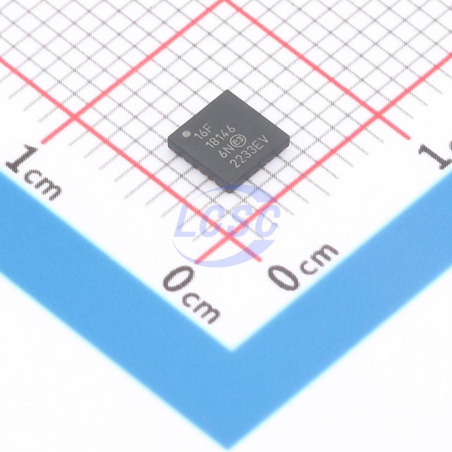
PIC16F18146-I/6N MICROCHIP
MICROCHIP

PIC16F18146-I/6N

PIC 8 Bit 32MHz VQFN-20(4x4) Microcontrollers RoHS

VQFN-20(4x4)ROHS3 CompliantActive

Full-Featured 14/20-Pin Microcontrollers

Manufacturer
MICROCHIP
Manufacturer part #
PIC16F18146-I/6N
Store part #
C5239521
Package / case
VQFN-20(4x4)
Packaging
Tube-packed
Datasheet (PDF)

Every Order Guarantee

100% Authentic · 30-Day Return or Replacement · policy

21 in stock

#C5239521

Stock & price checked 3 days ago

QuantityUnit pricePack price
1+₹174.46₹174.46
10+₹170.11₹1,701.10
30+₹167.07₹5,012.10
91+₹164.24₹14,945.84

1 × ₹174.46

₹174.46

excl. GST

₹205.86 incl. 18% GST

Need volume or a scheduled delivery? Request a quote
  • Dispatch in 15-18 working days
  • GST invoice with every order
  • Standard pack: 91 per tube

PIC16F18146-I/6N

₹174.46 for 1 + GST

Need this with the rest of your board? Upload the BOM — we price every line.Upload BOM

Specifications

DAC (Bit)
8bit
ADC (Bit)
12bit
Number of I/O
17
Operating Temperature
-40℃~+85℃
Program Memory Type
FLASH
Voltage - Supply
1.8V~5.5V
Program Storage Size
28KB
CPU Core
PIC
Core Size
8 Bit
CPU Maximum Speed
32MHz
Oscillator Type
Built-in

Packaging & compliance

RoHS
ROHS3 Compliant
Lifecycle
Active
ECCN
3A991A2
Packaging
Tube-packed
Standard pack
91 / Tube
Sold per
Piece
Minimum order
1
Unit weight
0.187 g

Overview

The PIC16F181 microcontroller family has a suite of analog peripherals that enables precision sensor applications. This product family is available from 8 to 44 - pin packages in a memory range of 7 KB to 28 KB, with speeds up to 32 MHz. This product includes a 12 - bit differential Analog - to - Digital Converter with Computation (ADCC), two 8 - bit Digital - to - Analog Converters (DAC), a 16 - bit Pulse - Width Modulation (PWM) peripheral, and many more waveform control and communication peripherals. This small form factor, feature - rich device is well suited for low - cost, energy - efficient analog sensor applications with higher resolution requirements.

Key features

  • C Compiler Optimized RISC Architecture
  • Operating Speed:
  • DC – 32 MHz clock input
  • 125 ns minimum instruction time
  • 16 - Level Deep Hardware Stack
  • Low - Current Power - on Reset (POR)
  • Configurable Power - up Timer (PWRT)
  • Brown - out Reset (BOR)
  • Low - Power Brown - out Reset (LPBOR)
  • Windowed Watchdog Timer (WWDT)
  • Up to 28 KB of Program Flash Memory
  • Up to 2 KB of Data SRAM Memory
  • Up to 256 Bytes of Data EEPROM Memory
  • Memory Access Partition (MAP) with Program Flash Memory Partitioned into:
  • Application block
  • Boot block
  • Storage Area Flash (SAF) block
  • Programmable Code Protection and Write Protection
  • Device Information Area (DIA) Stores:
  • Temperature Indicator calibration coefficients
  • Fixed Voltage Reference (FVR) measurement data
  • Microchip Unique Identifier (MUI)
  • Device Characteristics Area (DCI) Stores:
  • Program/erase row sizes
  • Pin count details
  • Direct, Indirect, and Relative Addressing Modes
  • Operating Voltage Range: 1.8V to 5.5V
  • Temperature Range:
  • Industrial: - 40℃ to 85℃
  • Extended: - 40℃ to 125℃
  • Doze: CPU and Peripherals Running at Different Cycle Rates (typically CPU is lower)
  • Idle: CPU Halted While Peripherals Operate
  • Sleep:
  • Lowest power consumption
  • Reduce system electrical noise while performing ADC conversions
  • Peripheral Module Disable (PMD): Selectively Minimize the Active Power Consumption of Unused Peripherals
  • Low Power Mode Features:
  • Sleep current:
  • <900 nA typical @3V/25℃ (WDT enabled)
  • <600 nA typical @3V/25℃ (WDT disabled)
  • Operating current:
  • 48 μA typical @32 kHz, 3V/25℃
  • <1 mA typical @4 MHz, 5V/25℃
  • Two Capture/Compare/PWM (CCP) Modules:
  • 16 - bit resolution for Capture/Compare modes
  • 10 - bit resolution for PWM mode
  • Up to Four Pulse - Width Modulators (PWM):
  • 16 - bit resolution
  • Independent pulse outputs
  • External Reset Signal (ERS) inputs
  • Four Configurable Logic Cells (CLC): Integrated combinational and sequential logic
  • One Complimentary Waveform Generator (CWG):
  • Rising and falling edge dead - band control
  • Full - bridge, half - bridge, 1 - channel drive
  • Multiple signal sources
  • Programmable dead band
  • Fault - shutdown input
  • Up to Three 8 - Bit Timers (TMR2/4/6) with Hardware Limit Timer (HLT)
  • One Numerically Controlled Oscillator (NCO):
  • Generates true linear frequency control and increased frequency resolution
  • Input clock up to 64 MHz
  • Programmable CRC with Memory Scan:
  • Reliable data/program memory monitoring for Fail - Safe operation (e.g., Class B)
  • Calculate 32 - bit CRC over any portion of Program Flash Memory
  • Two Enhanced Universal Synchronous Asynchronous Receiver Transmitters (EUSART):
  • RS - 232, RS - 485, LIN compatible
  • Auto - wake - up on Start
  • Two Host Synchronous Serial Ports (MSSP):
  • Serial Peripheral Interface (SPI) mode
  • Chip Select Synchronization
  • Inter - Integrated Circuit (I²C) mode
  • 7/10 - bit Addressing modes
  • Peripheral Pin Select (PPS): Enables pin mapping of digital I/O
  • Device I/O Port Features:
  • Up to 35 I/O pins
  • One input - only pin
  • Individual I/O direction, open - drain, input threshold, slew rate, and weak pull - up control
  • Interrupt - on - Change (IOC) on up to 25 pins
  • One external interrupt pin
  • Differential Analog - to - Digital Converter with Computation (ADCC):
  • 12 - bit resolution
  • Up to 35 external positive input channels
  • Up to 17 external negative input channels
  • Seven internal input channels
  • Internal ADC oscillator (ADCRC)
  • Operates in Sleep
  • Selectable Auto - Conversion Trigger (ACT) sources
  • Two 8 - Bit Digital - to - Analog Converters (DAC):
  • Output available on up to two I/O pins
  • Internal connections to ADC and Comparators
  • Two Comparators (CMP):
  • Up to four external inputs
  • Configurable output polarity
  • External output via Peripheral Pin Select
  • Zero - Cross Detect (ZCD): Detect when AC signal on pin crosses ground
  • Two Fixed Voltage References (FVR):
  • Selectable 1.024V, 2.048V and 4.096V output levels
  • FVR1 internally connected to ADC
  • FVR2 internally connected to Comparator
  • High - Precision Internal Oscillator Block (HFINTOSC):
  • Selectable frequencies up to 32 MHz ±2% at calibration
  • Active Clock Tuning of HFINTOSC for improved accuracy
  • Internal 31 kHz Oscillator (LFINTOSC)
  • External 32 kHz Secondary Oscillator (SOSC)
  • External High - Frequency Clock Input:
  • Three Crystal/Resonator modes
  • Two External Clock (EC) Power modes
  • 4x PLL available for external sources
  • Fail - Safe Clock Monitor: Allows for operational recovery if the external clock source stops
  • Oscillator Start - up Timer (OST): Ensures the stability of crystal oscillator sources
  • In - Circuit Serial Programming™ (ICSP™)

Alternatives

Similar parts — check the datasheet before substituting.

PIC16F18046T-I/ML#C20297060MICROCHIP · QFN-20(4x4)₹202.82 · 285 in stockView
PIC16F17146-I/6N#C5239671MICROCHIP · VQFN-20(4x4)₹224.37 · 0 in stockView
PIC16F18046-I/ML#C5239704MICROCHIP · QFN-20(4x4)₹157.87 · 0 in stockView
PIC16F17146T-I/6N#C20297029MICROCHIP · VQFN-20(4x4)₹369.74 · 0 in stockView
PIC16F18046-E/ML#C20297056MICROCHIP · QFN-20(4x4)₹337.99 · 0 in stockView

Same category

More in Microcontrollers

View all