Varnitronics
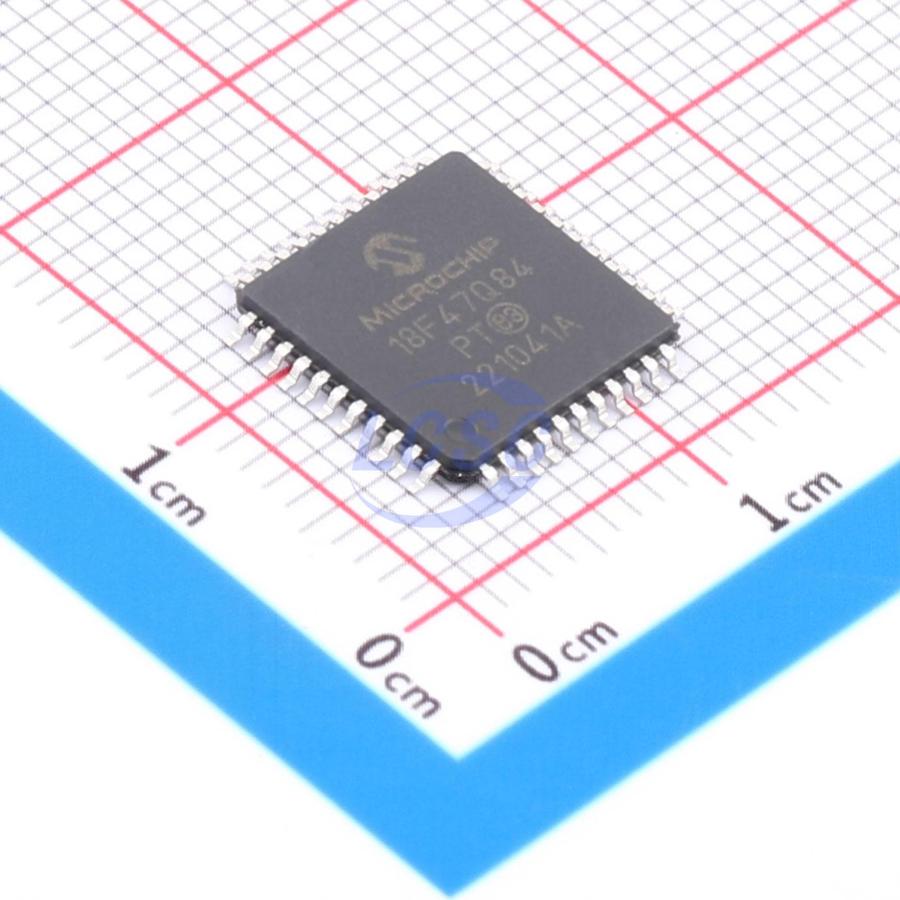
PIC18F47Q84-E/PT MICROCHIP
MICROCHIP

PIC18F47Q84-E/PT

PIC 8 Bit 64MHz VQFP-44(10x10) Microcontrollers RoHS

VQFP-44(10x10)ROHS3 CompliantActive

Low-Power, High-Performance Microcontroller with XLP Technology

Manufacturer
MICROCHIP
Manufacturer part #
PIC18F47Q84-E/PT
Store part #
C3226489
Package / case
VQFP-44(10x10)
Packaging
Tray
Datasheet (PDF)

Every Order Guarantee

100% Authentic · 30-Day Return or Replacement · policy

23 in stock

#C3226489

Stock & price checked 2 days ago

QuantityUnit pricePack price
1+₹580.59₹580.59
10+₹491.49₹4,914.90
30+₹438.48₹13,154.40
100+₹385.03₹38,503.00
500+₹360.25₹1,80,125.00
1,000+₹349.18₹3,49,180.00

1 × ₹580.59

₹580.59

excl. GST

₹685.10 incl. 18% GST

Need volume or a scheduled delivery? Request a quote
  • Dispatch in 15-18 working days
  • GST invoice with every order
  • Standard pack: 160 per tray

PIC18F47Q84-E/PT

₹580.59 for 1 + GST

Need this with the rest of your board? Upload the BOM — we price every line.Upload BOM

Specifications

DAC (Bit)
8bit
ADC (Bit)
12bit
Number of I/O
36
Operating Temperature
-40℃~+125℃
Program Memory Type
FLASH
Voltage - Supply
1.8V~5.5V
EEPROM
1KB
Program Storage Size
128KB
CPU Core
PIC
Core Size
8 Bit
CPU Maximum Speed
64MHz
Oscillator Type
Built-in

Packaging & compliance

RoHS
ROHS3 Compliant
Lifecycle
Active
ECCN
3A991A2
Packaging
Tray
Standard pack
160 / Tray
Sold per
Piece
Minimum order
1
Unit weight
1.364 g

Overview

The PIC18-Q84 microcontroller family is available in 28/40/44/48-pin devices for many automotive and industrial applications. The many communication peripherals found on the product family, such as Controller Area Network (CAN), Serial Peripheral Interface (SPI), Inter-Integrated Circuit (I²C), two Universal Asynchronous Receiver Transmitters (UARTs), can handle a wide range of wired and wireless (using external modules) communication protocols for intelligent applications. Combined with the Core Independent Peripherals (CIPs) integration capabilities, this capacity enables functions for motor control, power supply, sensor, signal and user interface applications. Additionally, this family includes a 12-bit Analog-to-Digital Converter (ADC) with Computation and Context Switching extensions for automated signal analysis to reduce the complexity of the application.

Applications

  • automotive applications
  • industrial applications

Key features

  • C Compiler Optimized RISC Architecture
  • Operating Speed: DC – 64 MHz clock input 62.5 ns minimum instruction cycle
  • Eight Direct Memory Access (DMA) Controllers:
  • Data transfers to SFR/GPR spaces from either Program Flash Memory, Data EEPROM or SFR/GPR spaces
  • User programmable source and destination sizes
  • Hardware and software triggered data transfers
  • Vectored Interrupt Capability:
  • Selectable high/low priority
  • Fixed interrupt latency of three instruction cycles
  • Programmable vector table base address
  • Backwards compatible with previous interrupt capabilities
  • 128-Level Deep Hardware Stack
  • Low-Current Power-on Reset (POR)
  • Configurable Power-up Timer (PWRT)
  • Brown-out Reset (BOR)
  • Low-Power BOR (LPBOR) Option
  • Windowed Watchdog Timer (WWDT):
  • Watchdog Reset on too long or too short interval between watchdog clear events
  • Variable prescaler selection
  • Variable window size selection
  • Up to 128 KB of Program Flash Memory
  • Up to 13 KB of Data SRAM Memory
  • 1024 Bytes Data EEPROM
  • Memory Access Partition: The Program Flash Memory can be partitioned into:
  • Application Block
  • Boot Block
  • Storage Area Flash (SAF) Block
  • Programmable Code Protection and Write Protection
  • Device Information Area (DIA) Stores:
  • Temperature indicator factory calibrated data
  • Fixed Voltage Reference measurement data
  • Microchip unique identifier
  • Device Characteristics Information (DCI) Area Stores:
  • Program/erase row sizes
  • Pin count details
  • EEPROM size
  • Direct, Indirect and Relative Addressing modes
  • Operating Voltage Range: 1.8V to 5.5V
  • Temperature Range:
  • Industrial: -40℃ to 85℃
  • Extended: -40℃ to 125℃
  • Doze: CPU and Peripherals Running at Different Cycle Rates (typically CPU is lower)
  • Idle: CPU Halted While Peripherals Operate
  • Sleep: Lowest Power Consumption
  • Peripheral Module Disable (PMD):
  • Ability to selectively disable hardware module to minimize active power consumption of unused peripherals
  • Low-Power Mode Features:
  • Sleep: <1μA typical @ 3V
  • Operating Current: 48μμ @ 32 kHz, 3V, typical
  • Four 16-Bit Pulse-Width Modulators (PWM):
  • Dual outputs for each PWM module
  • Integrated 16-bit timer/counter
  • Double-buffered user registers for duty cycles
  • Right/Left/Center/Variable aligned modes of operation
  • Multiple clock and Reset signal selections
  • Three 16-Bit Timers (TMR0/1/3)
  • Three 8-Bit Timers (TMR2/4/6) with Hardware Limit Timer (HLT)
  • Two Universal Timers (TMRU16A/16B):
  • New Timer modules with features of TMR0/TMR1/TMR2 (Gate, Hardware Limit)
  • Two 16-bit timers can be chained together to create a combined 32-bit timer
  • Eight Configurable Logic Cell (CLC):
  • Integrated combinational and sequential logic
  • Three Complimentary Waveform Generators (CWG):
  • Rising and falling edge dead-band control
  • Full-bridge, half-bridge, 1-channel drive
  • Multiple signal sources
  • Programmable dead band
  • Fault-shutdown input
  • Three Capture/Compare/PWM (CCP) Modules:
  • 16-bit resolution for Capture/Compare modes
  • 10-bit resolution for PWM mode
  • Three Numerically Controlled Oscillators (NCO):
  • Generates true linear frequency control and increased frequency resolution
  • Input clock up to 64 MHz
  • Signal Measurement Timer (SMT):
  • 24-bit timer/counter with prescaler
  • Several modes of operation like Time-of-Flight, Period and Duty Cycle measurement, etc.
  • Data Signal Modulator (DSM):
  • Multiplex two carrier clocks, with glitch prevention feature
  • Multiple sources for each carrier
  • Programmable CRC with Memory Scan:
  • Reliable data/program memory monitoring for Fail-Safe operation (e.g., Class B)
  • Calculate 16-bit CRC over any portion of Program Flash Memory
  • CAN Flexible Data-Rate (FD) Module:
  • Functional in CAN FD or CAN 2.0B modes
  • One dedicated transmit FIFO
  • Three programmable transmit/receive FIFOs
  • One transmit event queue
  • 12 acceptance masks/filters
  • Five UART Modules:
  • LIN host and client, DMX mode, DALI gear and device protocols
  • Asynchronous UART, RS-232, RS-485 compatible
  • Automatic and user timed BREAK period generation
  • Automatic checksums
  • Programmable 1, 1.5, and two Stop bits
  • Wake-up on BREAK reception
  • DMA compatible
  • Two SPI Modules:
  • Configurable length bytes
  • Arbitrary length data packets
  • Transmit-without-receive and receive-without-transmit options
  • Transfer byte counter
  • Separate transmit and receive buffers with 2-byte FIFO and DMA capabilities
  • One I²C module, SMBus, PMBus Compatible:
  • 7-bit and 10-bit Addressing modes with Address Masking modes
  • Dedicated address, transmit and receive buffers and DMA capabilities
  • Bus collision detection with arbitration
  • Bus time-out detection and handling
  • I2C, SMBus 2.0 and SMBus 3.0, and 1.8V input level selections
  • Multi-Host mode, including self-addressing
  • Device I/O Port Features:
  • 25 I/O pins (PIC18F26/27Q84)
  • 36 I/O pins (PIC18F46/47Q84)
  • 44 I/O pins (PIC18F5

Alternatives

Similar parts — check the datasheet before substituting.

PIC18F47Q84-I/PT#C2987161MICROCHIP · TQFP-44(10x10)₹685.78 · 35 in stockView
PIC18F47K42-E/PT#C634540MICROCHIP · TQFP-44(10x10)₹726.50 · 7 in stockView
PIC18F47K42T-I/PT#C630876MICROCHIP · TQFP-44(10x10)₹568.18 · 1 in stockView
PIC18F47K42-I/PT#C634541MICROCHIP · TQFP-44(10x10)₹633.08 · 32 in stockView
PIC18F47Q10-E/PT#C634542MICROCHIP · TQFP-44(10x10)₹343.23 · 4 in stockView

Same category

More in Microcontrollers

View all