Varnitronics
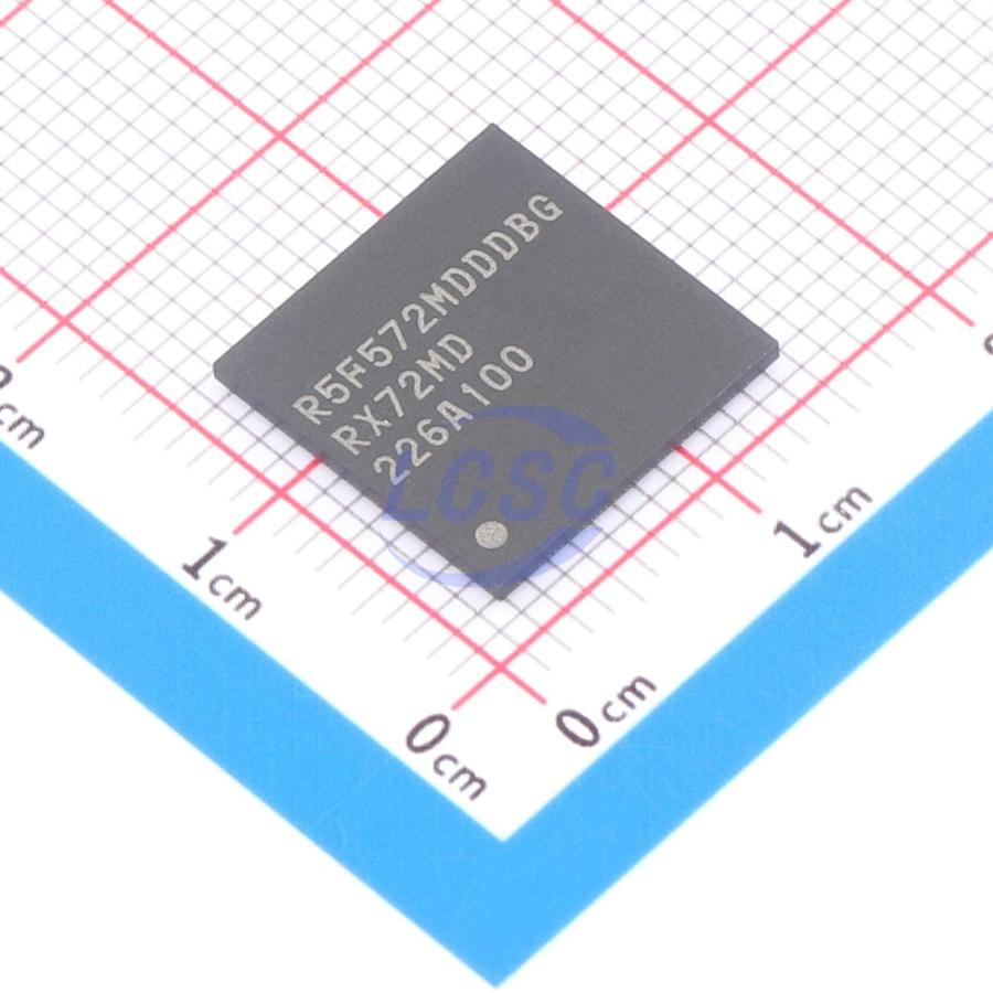
R5F572MDDDBG#20 RENESAS
RENESAS

R5F572MDDDBG#20

RXv3 32 Bit 240MHz LFBGA-176 Microcontrollers RoHS

LFBGA-176ROHS3 CompliantActive

240-MHz 32-bit RX MCU, on-chip double-precision FPU, EtherCAT Slave Controller, various communications interfaces

Manufacturer
RENESAS
Manufacturer part #
R5F572MDDDBG#20
Store part #
C1018668
Package / case
LFBGA-176
Packaging
Tray
Datasheet (PDF)

Every Order Guarantee

100% Authentic · 30-Day Return or Replacement · policy

5 in stock

#C1018668

Stock & price checked 24 h ago

QuantityUnit pricePack price
1+₹3,556.41₹3,556.41
10+₹3,439.99₹34,399.90

1 × ₹3,556.41

₹3,556.41

excl. GST

₹4,196.56 incl. 18% GST

Need volume or a scheduled delivery? Request a quote
  • Dispatch in 15-18 working days
  • GST invoice with every order
  • Standard pack: 152 per tray

R5F572MDDDBG#20

₹3,556.41 for 1 + GST

Need this with the rest of your board? Upload the BOM — we price every line.Upload BOM

Specifications

DAC (Bit)
12bit
ADC (Bit)
12bit
Number of I/O
136
Operating Temperature
-40℃~+85℃
Voltage - Supply
2.7V~3.6V
Program Memory Type
FLASH
EEPROM
32KB
Program Storage Size
2MB
CPU Core
RXv3
Core Size
32 Bit
CPU Maximum Speed
240MHz
Oscillator Type
Built-in

Packaging & compliance

RoHS
ROHS3 Compliant
Lifecycle
Active
ECCN
3A991A2
Packaging
Tray
Standard pack
152 / Tray
Sold per
Piece
Minimum order
1
Unit weight
5.84 g

Overview

Key features

  • 32-bit RXv3 CPU core
  • Maximum operating frequency: 240 MHz
  • Capable of 1396 CoreMark in operation at 240 MHz
  • Double-precision 64-bit IEEE-754 floating point
  • A collective register bank save function is available.
  • Supports the memory protection unit (MPU)
  • JTAG and FINE (one-line) debugging interfaces
  • Low-power design and architecture
  • Operation from a single 2.7- to 3.6-V supply
  • RTC is capable of operation from a dedicated power supply.
  • Four low-power modes
  • On-chip code flash memory
  • Supports versions with up to 4 Mbytes of ROM
  • No wait cycles at up to 120 MHz or when the ROM cache is hit, one-wait state at above 120 MHz
  • User code is programmable by on-board or off-board programming.
  • Programming/erasing as background operations (BGOs)
  • A dual-bank structure allows exchanging the start-up bank.
  • On-chip data flash memory
  • 32 Kbytes, reprogrammable up to 100,000 times
  • Programming/erasing as background operations (BGOs)
  • On-chip SRAM
  • 1 Mbyte of SRAM (no wait states; however, if ICLK is at a frequency above 120 MHz, access to locations in the 512 Kbytes of SRAM from 0080 0000h to 0087 FFFFh requires one cycle of waiting)
  • 32 Kbytes of RAM with ECC (single error correction/double error detection)
  • 8 Kbytes of standby RAM (backup on deep software standby)
  • Data transfer
  • DMACAa: 8 channels
  • DTCb: 1 channel
  • EXDMAC: 2 channels
  • DMAC for the Ethernet controller: 3 channels
  • Reset and supply management
  • Power-on reset (POR)
  • Low voltage detection (LVD) with voltage settings
  • Clock functions
  • External crystal resonator or internal PLL for operation at 8 to 24 MHz
  • PLL for specific purposes
  • Internal 240-kHz LOCO and HOCO selectable from 16, 18, and 20 MHz
  • 120-kHz clock for the IWDTa
  • Real-time clock
  • Adjustment functions (30 seconds, leap year, and error)
  • Real-time clock counting and binary counting modes are selectable
  • Time capture function (for capturing times in response to event-signal input)
  • Independent watchdog timer
  • Useful functions for IEC60730 compliance
  • Oscillation-stoppage detection, frequency measurement, CRCA, IWDTa, self-diagnostic function for the A/D converter, etc.
  • Register write protection function can protect values in important registers against overwriting.
  • Various communications interfaces
  • EtherCAT slave controller (two ports)
  • Ethernet MAC compliant with IEEE 1588 (2 channels)
  • PHY layer (1 channel) for host/function or OTG controller (1 channel) with full-speed USB 2.0 transfer
  • CAN (compliant with ISO11898-1), incorporating 32 mailboxes (3 channels)
  • SCIj and SCIh with multiple functionalities (8 channels) Choose from among asynchronous mode, clock-synchronous mode, smart-card interface mode, simplified SPI, simplified I2C, and extended serial mode.
  • SCIi with 16-byte transmission and reception FIFOs (5 channels)
  • I²C bus interface for transfer at up to 1 Mbps (3 channels)
  • Four-wire QSPI (1 channel) in addition to RSPIc (3 channels)
  • Parallel data capture unit (PDC) for the CMOS camera interface
  • Graphic-LCD controller (GLCDC)
  • 2D drawing engine (DRW2D)
  • SD host interface (1 channel) with a 1- or 4-bit SD bus for use with SD memory or SDIO
  • MMCIF with 1-, 4-, or 8-bit transfer bus width
  • External address space
  • Buses for full-speed data transfer (max. operating frequency of 80 MHz)
  • 8 CS areas
  • 8-, 16-, or 32-bit bus space is selectable per area
  • Independent SDRAM area (128 Mbytes)
  • Up to 29 extended-function timers
  • 32-bit GPTW (4 channels)
  • 16-bit TPUa (6 channels), MTU3a (9 channels)
  • 8-bit TMRa (4 channels), 16-bit CMT (4 channels), 32-bit CMTW (2 channels)
  • 12-bit A/D converter
  • Two 12-bit units (8 channels for unit 0; 21 channels for unit 1)
  • Self diagnosis, detection of analog input disconnection

Alternatives

Similar parts — check the datasheet before substituting.

R5F572MNDDBG#20#C1015361RENESAS · LFBGA-176₹2,037.82 · 0 in stockView
R5F572NDDDBG#20#C1018625RENESAS · LFBGA-176₹1,939.72 · 0 in stockView
R5F572NNHDBG#20#C1018639RENESAS · LFBGA-176₹2,105.53 · 0 in stockView
R5F572MNHDBG#20#C1018650RENESAS · LFBGA-176₹2,303.81 · 0 in stockView
R5F572NNDDBG#20#C1018656RENESAS · LFBGA-176₹2,044.67 · 0 in stockView

Same category

More in Microcontrollers

View all