Varnitronics
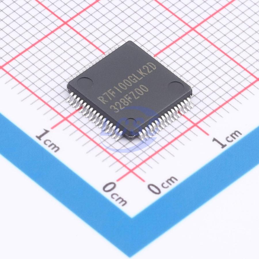
R7F100GLK2DFB#BA0 RENESAS
RENESAS

R7F100GLK2DFB#BA0

RL78 16 Bit 32MHz LFQFP-64(10x10) Microcontrollers RoHS

LFQFP-64(10x10)ROHS3 CompliantActive

True low-power platform, operating current, data retention current, code flash memory, RAM, capacitive sensing unit, pins, power supply voltage

Manufacturer
RENESAS
Manufacturer part #
R7F100GLK2DFB#BA0
Store part #
C20353280
Package / case
LFQFP-64(10x10)
Packaging
Tray
Datasheet (PDF)

Every Order Guarantee

100% Authentic · 30-Day Return or Replacement · policy

8 in stock

#C20353280

Stock & price checked 40 h ago

QuantityUnit pricePack price
1+₹637.32₹637.32
10+₹622.27₹6,222.70
30+₹612.39₹18,371.70
100+₹602.51₹60,251.00

1 × ₹637.32

₹637.32

excl. GST

₹752.04 incl. 18% GST

Need volume or a scheduled delivery? Request a quote
  • Dispatch in 15-18 working days
  • GST invoice with every order
  • Standard pack: 1,280 per tray

R7F100GLK2DFB#BA0

₹637.32 for 1 + GST

Need this with the rest of your board? Upload the BOM — we price every line.Upload BOM

Specifications

Number of I/O
54
Operating Temperature
-40℃~+85℃
Program Memory Type
FLASH
Voltage - Supply
1.6V~5.5V
EEPROM
8KB
Program Storage Size
384KB
CPU Core
RL78
Core Size
16 Bit
CPU Maximum Speed
32MHz
Oscillator Type
Built-in

Packaging & compliance

RoHS
ROHS3 Compliant
Lifecycle
Active
ECCN
3A991A2
Packaging
Tray
Standard pack
1,280 / Tray
Sold per
Piece
Minimum order
1
Unit weight
9.48 g

Overview

True low-power platform, 41 - μA/μHz operating current, 210-nA data retention current for 4 KB of RAM, up to 768-KB code flash memory and 48-KB RAM, capacitive sensing unit, from 30 to 128 pins, 1.6 - 5.5 V

Key features

  • Ultra-low power consumption technology
  • VDD: single power supply voltage of 1.6 to 5.5 V
  • HALT mode
  • STOP mode
  • High-speed wakeup from the STOP mode is possible.
  • SNOOZE mode
  • RL78 CPU core: CISC architecture with 3-stage pipeline
  • Minimum instruction execution time: Can be changed from high speed (0.03125 μs @ 32 MHz operation with the high - speed on - chip oscillator clock) to ultra - low speed (30.5 μs @ 32.768 kHz operation with the subsystem clock)
  • Multiply/divide/multiply & accumulate instructions are supported.
  • Address space: 1 MB
  • General - purpose registers: (8 - bit register × 8) × 4 banks
  • On - chip RAM: 12 to 48 KB
  • Code flash memory: 96 to 768 KB
  • Block size: 2 KB
  • Prohibition of block erase and rewriting (security function)
  • On - chip debugging
  • Self - programming (with boot swapping and flash shield window)
  • Data flash memory: 8 KB
  • Background operation (BGO): Instructions can be executed from the program memory while rewriting the data flash memory.
  • Number of rewrites: 1,000,000 times (typ.)
  • High - speed on - chip oscillator: Select from 32 MHz, 24 MHz, 16 MHz, 12 MHz, 8 MHz, 6 MHz, 4 MHz, 3 MHz, 2 MHz, or 1 MHz
  • High accuracy: ±1.0% (VDD = 1.8 to 5.5 V, TA = - 20 to + 85 ℃)
  • Middle - speed on - chip oscillator: Select from 4 MHz, 2 MHz, or 1 MHz (with adjustability)
  • Low - speed on - chip oscillator: 32.768 kHz (typ.) (with adjustability)
  • Operating ambient temperature: TA = - 40 to + 85 ℃ (2D: Consumer applications); TA = - 40 to + 105 ℃ (3C: Industrial applications)
  • Power management and reset function: On - chip power - on - reset (POR) circuit; On - chip voltage detectors (LVD0 and LVD1)
  • Data transfer controller (DTC): Transfer modes: Normal transfer mode, repeat transfer mode, block transfer mode; Activation sources: Activated by interrupt sources; Chain transfer function
  • SNOOZE mode sequencer (SMS): Calculations and comparison of values by the commands for use in processing by the sequencer can realize intermittent operations where the RL78/G23 does not have to return to normal operation.
  • Sequentially handling a total of 32 processes with the use of desired commands from among 21 different ones
  • The SNOOZE mode sequencer offers operation with low power consumption without using the CPU, flash memory, and RAM.
  • Logic and event link controller (ELCL): Event signals can be set up between specified peripheral functions.
  • The signals can be generated by the input of multiple event signals to the logic circuit.
  • Flip - flop circuits are incorporated to handle setting and resetting functions.
  • Serial interface: Simplified SPI (CSINote 1): 3 to 8 channels; UART/UART (LIN - bus supported)/UARTA: 3 to 6 channels; I2C/Simplified I2C: 4 to 10 channels
  • Remote control signal receiver: 1 channel; Matching of 4 waveform patterns (header, data 0, data 1, and special data)
  • Timers: 16 - bit timer: 8 to 16 channels; 32 - bit interval timer: 1 channel in 32 - bit counter mode, 2 channels in 16 - bit counter mode, 4 channels in 8 - bit counter mode; Realtime clock: 1 channel (counting of one second to 99 years, alarm interrupt, and clock correction); Watchdog timer: 1 channel (operates with the dedicated low - speed on - chip oscillator clock)
  • A/D converter: 8 -/10 -/12 - bit resolution A/D converter; Analog input: 8 to 26 channels; Internal reference voltage (1.48 V) and temperature sensor
  • D/A converter: 8 - bit resolution D/A converter; Analog output: 2 channels; Output voltage: 0 V to VDD; Realtime output function
  • Comparator: 2 channels; Operating modes: Comparator high - speed mode and comparator low - speed mode; The external reference voltage and the internal reference voltage or D/A converter output are selectable as the reference voltage.
  • Capacitive sensing unit: CTSU2L operating voltage condition: VDD = 1.8 to 5.5 V; Self - capacitance method: A single pin configures a single key, supporting up to 32 keys; Mutual capacitance method: Matrix configuration with 8 × 8 pins, supporting up to 64 keys
  • Input/output port pins: Number of port pins: 26 to 120 (N - ch open drain I/O [withstand voltage of 6 V]: 2 to 4, N - ch open drain I/O [VDD withstand voltageNote 2/EVDD withstand voltageNote 3]: 10 to 33, output current control pins: 6 to 8); Can be set to N - ch open drain or TTL input buffer, and use of an on - chip pull - up resistor can be specified.
  • Connectable to a device with different voltage (1.8, 2.5, or 3 V)
  • Others: Key interrupt input; Clock output/buzzer output controller; BCD (binary - coded decimal) correction circuit

Alternatives

Similar parts — check the datasheet before substituting.

R7F100GLK2DFB#HA0#C20353281RENESAS · LFQFP-64(10x10)₹797.41 · 0 in stockView
R7F100GLK3CFB#BA0#C20353287RENESAS · LFQFP-64(10x10)₹855.39 · 0 in stockView
R7F100GLK3CFB#HA0#C20353288RENESAS · LFQFP-64(10x10)₹850.89 · 0 in stockView
R7F100GLL2DFB#BA0#C20353294RENESAS · LFQFP-64(10x10)₹918.65 · 0 in stockView
R7F100GLL2DFB#HA0#C20353295RENESAS · LFQFP-64(10x10)₹913.95 · 0 in stockView

Same category

More in Microcontrollers

View all