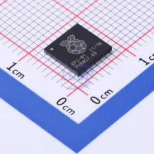
STC Micro
STC8H1K08-36I-TSSOP2051 Series 8 Bit 33MHz TSSOP-20 Microcontrollers RoHS
From
₹42.36
1,35,660 in stock
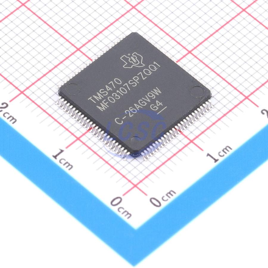
ARM Cortex-M3 32 Bit 80MHz LQFP-100(14x14) Microcontrollers RoHS
16/32-bit Reduced Instruction Set Computing (RISC) flash microcontroller
Every Order Guarantee
100% Authentic · 30-Day Return or Replacement · policy
10 in stock
#C1337743
Stock & price checked 6 days ago
| Quantity | Unit price | Pack price |
|---|---|---|
| 1+ | ₹1,190.83 | ₹1,190.83 |
| 10+ | ₹1,162.76 | ₹11,627.60 |
| 30+ | ₹1,144.20 | ₹34,326.00 |
| 100+ | ₹1,125.41 | ₹1,12,541.00 |
1 × ₹1,190.83
₹1,190.83
excl. GST
₹1,405.18 incl. 18% GST
S4MF03107SPZQQ1
₹1,190.83 for 1 + GST
The TMS470MF04207/03107 devices belong to the TMS470M automotive-grade 16/32-bit Reduced Instruction Set Computer (RISC) microcontroller family. The TMS470M microcontrollers leverage the high-efficiency Cortex–M3 16/32-bit RISC Central Processing Unit (CPU) to deliver high performance, thereby achieving high instruction throughput and maintaining excellent code efficiency. The TMS470M devices use the big-endian byte order format, in which the most significant byte of a word is stored in the lowest-numbered byte, while the least significant byte is stored in the highest-numbered byte. High-end embedded control applications require their controllers to provide more performance while keeping costs low. The TMS470M microcontroller architecture provides a solution for these performance and cost requirements while maintaining low power consumption. The composition of the TMS470MF04207/03107 devices is as follows: - 16/32-bit RISC CPU core - Up to 448K bytes of program flash memory (with SECDED ECC) for TMS470MF04207 - Up to 320K bytes of program flash memory (with SECDED ECC) for TMS470MF03107 - 64K bytes of flash memory (with SECDED ECC) for additional program space or EEPROM emulation - Up to 24K bytes of Static RAM (SRAM) (with SECDED ECC) - Real-Time Interrupt Timer (RTI) - Vector Interrupt Module (VIM) - Hardware Built-In Self-Test (BIST) checker for SRAM (MBIST) and CPU (LBIST) - 64-bit Cyclic Redundancy Checker (CRC) - Clock module based on Frequency-Modulated Zero-Pin Phase-Locked Loop (FMzPLL) (with pre-scaler) - Two Multi-Buffered Serial Peripheral Interfaces (MibSPI) - Two UARTs (SCI) with Local Interconnect Network Interface (LIN) - Two CAN controllers (DCAN) - High-End Timer (HET) - External Clock Pre-Scaler (ECP) module - One 16-channel 10-bit Multi-Buffered ADC (MibADC) - Error Signaling Module (ESM) - 4 dedicated General-Purpose I/O (GIO) pins and 45 additional peripheral I/O (100-pin package) The TMS470M memory includes general-purpose SRAM, which supports single-cycle read/write access in byte, half-word, and word modes. The SRAM on the TMS470M devices can be protected using ECC. This feature uses a single-error correction and double-error detection circuit (SECDED circuit) to detect and selectively correct single-bit errors and detect all double-bit errors and some multi-bit errors. This is achieved by storing an 8-bit ECC checksum/code for each 64-bit double-word of the memory space in a separate ECC RAM memory space. The flash memory on the device is a non-volatile, electrically erasable, and programmable memory. It is implemented using a 144-bit wide data word (128 bits without ECC) and a 64-bit wide flash module interface. The flash memory operates at a system clock frequency of up to 28MHz. The pipeline mode with flash data linear prefetching enables a system clock of up to 80MHz. The Enhanced Real-Time Interrupt (RTI) module on the TMS470M devices can be optionally driven by the oscillator clock. The Digital Watchdog (DWD) is a 25-bit resettable down-counter that provides a system reset when the watchdog counter expires. The TMS470M devices have six communication interfaces: two LIN/SCI, two DCAN, and two MibSPI. LIN is the Local Interconnect Network standard and also supports an SCI mode. SCI can be used in a full-duplex, serial I/O interface for asynchronous communication between the CPU and other peripherals using the standard Non-Return-to-Zero (NRZ) format. DCAN uses a serial, multi-master communication protocol that efficiently supports distributed real-time control and robust communication rates of up to 1 Megabit per second (Mbps). DCAN is well-suited for applications operating in noisy and harsh environments (e.g., automotive and industrial fields) that require reliable serial communication or multiplexed lines. MibSPI provides a convenient serial interaction method for high-speed communication between similar shift register-type devices. MibSPI provides standard SOMI, SIMO, and SPI clock interfaces as well as up to 8 chip select lines. HET is an advanced intelligent timer that provides precise timing functions for real-time applications. The timer is software-controlled, uses a reduced instruction set, and has a dedicated micro-timer and a connected I/O port. This HET can be used for comparison, capture, or general-purpose I/O. It is particularly suitable for applications that require multiple sensor information and actuator driving with complex and accurate time pulses. The TMS470M HET peripheral includes an "Exclusive OR (XOR) sharing" function. This function allows the "XOR" operation of two adjacent HET high-resolution channels, enabling the output of a pulse smaller than the standard HET. The TMS470M devices have a 10-bit resolution sample-and-hold MibADC. Each MibADC channel can be grouped using software for sequential conversion sequences. There are three separate groups, all of which can be triggered by an external event. Each sequence can perform a single conversion when triggered or be configured to operate in continuous conversion mode. The Frequency-Modulated Zero-Pin Phase-Locked Loop (FMzPLL) clock module includes a phase-locked loop, a clock monitor circuit, a clock enable circuit, and a pre-scaler. The function of the FMzPLL is to multiply the external frequency reference to a higher frequency for internal use. The FMzPLL provides the input to the Global Clock Module (GCM). The GCM module then provides the system clock (HCLK), real-time interrupt clock (RTICLK), CPU clock (GCLK), HET clock (VCLK2), DCAN clock (AVCLK1), and peripheral interface clock (VCLK) to all other TMS470M device modules. In addition, the TMS470MF04207/TMS470MF03107 devices also have two External Clock Pre-Scaler (ECP) modules, which output a continuous external clock (ECLK) when enabled. The ECLK1 frequency is a user-programmable ratio of the peripheral interface clock (VCLK) frequency. The second ECLK output can be selected to replace the HET15 output. It shares the same source clock as ECLK1 but can be independently configured for a separate output frequency derived from ECLK1. The Error Signaling Module (ESM) provides a common location for error reporting within the device, enabling efficient error checking and identification.
Similar parts — check the datasheet before substituting.
| Part | Manufacturer | Package | Stock | Price from (excl. GST) | Action | |
|---|---|---|---|---|---|---|
 | S4MF03107SPZQQ1R#C2056785TI · LQFP-100(14x14) | TI | LQFP-100(14x14) | 5 | ₹1,721.87 · 5 in stock | View |
 | S4MF06607BSPZQQ1#C2863770TI · LQFP-100(14x14) | TI | LQFP-100(14x14) | 2 | ₹1,913.22 · 2 in stock | View |
| S4MF04207SPZQQ1#C1341091TI · LQFP-100(14x14) | TI | LQFP-100(14x14) | On request | ₹2,273.83 · 0 in stock | View | |
Same category
STC Micro
STC8H1K08-36I-TSSOP2051 Series 8 Bit 33MHz TSSOP-20 Microcontrollers RoHS
From
₹42.36
1,35,660 in stock
STC Micro
STC8G1K08A-36I-SOP851 Series 8 Bit 36MHz SOP-8 Microcontrollers RoHS
From
₹35.85
82,120 in stock
PUYA
PY32F002BF15U6TRARM Cortex-M0+ 32 Bit 24MHz QFN-20-EP(3x3) Microcontrollers
From
₹23.27
77,720 in stock
Raspberry Pi
RP2040ARM Cortex-M0+ 32 Bit 133MHz LQFN-56(7x7) Microcontrollers
From
₹143.45
68,116 in stock
SILICON LABS
EFM8BB21F16G-C-QFN20R51 Series 8 Bit 50MHz QFN-20-EP(3x3) Microcontrollers RoHS
From
₹167.39
59,930 in stock