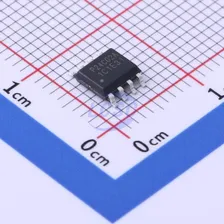
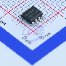
Every Order Guarantee
100% Authentic · 30-Day Return or Replacement · policy
40 in stock
#C17627475
Stock & price checked 3 days ago
| Quantity | Unit price | Pack price |
|---|---|---|
| 1+ | ₹1,855.88 | ₹1,855.88 |
| 10+ | ₹1,605.66 | ₹16,056.60 |
| 30+ | ₹1,453.21 | ₹43,596.30 |
| 100+ | ₹1,325.38 | ₹1,32,538.00 |
1 × ₹1,855.88
₹1,855.88
excl. GST
₹2,189.94 incl. 18% GST
- Dispatch in 15-18 working days
- GST invoice with every order
- Standard pack: 338 per tray
S80KS5122GABHI020
₹1,855.88 for 1 + GST
Specifications
- Refresh Current
- 40mA
Packaging & compliance
- RoHS
- ROHS3 Compliant
- Lifecycle
- Active
- ECCN
- 3A991B1A
- Packaging
- Tray
- Standard pack
- 338 / Tray
- Sold per
- Piece
- Minimum order
- 1
- Unit weight
- 1.99 g
Overview
The 512 Mb HYPERRAM™ device is a high-speed CMOS self-refresh dynamic random access memory (DRAM) with a HYPERBURST™ interface. The DRAM array uses dynamic cells that require periodic refresh. When the HYPERBURST™ interface master (host) is not actively reading from or writing to the memory, the refresh control logic within the device manages the refresh operations of the DRAM array. Since the host does not need to manage any refresh operations, the DRAM array appears to the host as a memory using static cells that retain data without requiring refresh. Therefore, this memory is more accurately described as pseudo-static random access memory (PSRAM). Because DRAM cells cannot be refreshed during read and write transactions, the host is required to limit read and write burst transfer lengths to allow internal logic refresh operations when needed. If the memory indicates that a refresh operation is required, the host must limit the duration of the transaction and allow additional initial access latency at the start of a new transaction.
Key features
- Interface:
- HyperBus™ interface support
- 1.8 V interface support
- Single-ended clock (CK) - 11 bus signals
- Optional differential clock (CK, CK#) - 12 bus signals
- Chip Select (CS#)
- 8-bit data bus (DQ[7:0])
- Hardware Reset (RESET#)
- Read/Write Data Strobe (RWDS), bidirectional
- Output at the start of all transactions to indicate refresh latency
- Output as read data strobe during read transactions
- Input as write data mask during write transactions
- Performance, Power, and Package:
- Maximum clock frequency 200 MHz
- DDR - data transfer on both edges of the clock
- Data throughput up to 400 MBps (3,200 Mbps)
- Configurable burst characteristics
- Linear burst
- Wrapped burst lengths: 16 bytes (8 clocks), 32 bytes (16 clocks), 64 bytes (32 clocks), 128 bytes (64 clocks)
- Hybrid option - one wrapped burst followed by linear burst on 256 Mb; linear burst across die boundary not supported
- Configurable output drive strength
- Power modes: Hybrid Sleep, Deep Power-Down
- Array refresh: partial memory array (1/8, 1/4, 1/2, etc.), full array
- Package: 24-ball FBGA
- Operating temperature range: Industrial (I): -40°C to +85°C; Industrial Plus (V): -40°C to +105°C; Automotive, AEC-Q100 Grade 3: -40°C to +85°C; Automotive, AEC-Q100 Grade 2: -40°C to +105°C; Automotive, AEC-Q100 Grade 1: -40°C to +125°C
- Technology: 25 nm DRAM
Same category