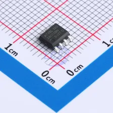
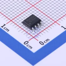
SST39VF040704ITU
4Mbit 2.7V~3.6V Parallel TSOP-32 Memory RoHS
Every Order Guarantee
100% Authentic · 30-Day Return or Replacement · policy
34 in stock
#C43651917
Stock & price checked 17 h ago
| Quantity | Unit price | Pack price |
|---|---|---|
| 1+ | ₹740.83 | ₹740.83 |
| 10+ | ₹637.42 | ₹6,374.20 |
| 30+ | ₹575.94 | ₹17,278.20 |
| 234+ | ₹513.59 | ₹1,20,180.06 |
| 468+ | ₹484.91 | ₹2,26,937.88 |
| 936+ | ₹472.10 | ₹4,41,885.60 |
1 × ₹740.83
₹740.83
excl. GST
₹874.18 incl. 18% GST
- Dispatch in 15-18 working days
- GST invoice with every order
- Standard pack: 234 per bag
SST39VF040704ITU
₹740.83 for 1 + GST
Specifications
- Operating Temperature
- -40℃~+85℃
- Features
- Hardware write protection;Software write protection
- Memory Size
- 4Mbit
- Voltage - Supply
- 2.7V~3.6V
- Program / Erase Cycles
- 10000 times
- Data Retention - TDR (Year)
- 100 Years
- Standby Supply Current
- 15uA
- Interface
- Parallel
Packaging & compliance
- RoHS
- ROHS Compliant
- Lifecycle
- Active
- Packaging
- Bag-packed
- Standard pack
- 234 / Bag
- Sold per
- Piece
- Minimum order
- 1
- Unit weight
- 1.84 g
Overview
The SST39LF010/020/040 and SST39VF010/020/040 devices are CMOS multi-purpose Flash memory organized as 128K×8, 256K×8, and 512K×8, manufactured using proprietary high-performance CMOS SuperFlash technology. Their split-gate cell design and thick-oxide tunneling injector deliver superior reliability and manufacturability compared to alternative approaches. The SST39LF010/020/040 devices perform write operations at a VCC supply voltage of 3.0V to 3.6V, while the SST39VF010/020/040 devices operate at 2.7V to 3.6V. These devices comply with the JEDEC standard x8 memory pin assignment specification. With high-performance byte-program capability, these devices offer a maximum byte-program time of 20 μs. They use toggle bit or data polling to indicate completion of program operations. To prevent inadvertent writes, on-chip hardware and software data protection mechanisms are integrated. These devices are designed, manufactured, and tested for a broad range of applications, with a typical endurance of 100,000 erase/program cycles and a data retention period exceeding 100 years. These devices are suited for applications requiring convenient and cost-effective updates to program, configuration, or data memory. Across all system applications, they deliver significant improvements in performance and reliability while reducing power consumption. During erase and program operations, the inherent power consumption is lower than that of other Flash technologies. Total energy consumption is a function of the applied voltage, current, and duration. Since SuperFlash technology requires less current for programming and achieves shorter erase times within a given voltage range, the total energy dissipated per erase or program operation is lower than that of other Flash technologies. These devices also enhance flexibility while reducing cost in program, data, and configuration storage applications. SuperFlash technology provides fixed erase and program times, independent of the number of erase/program cycles that have occurred. As a result, no system software or hardware modifications or derating are required, unlike other Flash technologies whose erase and program times increase with accumulated erase/program cycles.
Key features
- Organization: 128K×8 / 256K×8 / 512K×8
- Single voltage read/write operation: 3.0V~3.6V for SST39LF010/020/040; 2.7V~3.6V for SST39VF010/020/040
- High reliability: 100,000 typical erase/write cycles; data retention greater than 100 years
- Low power consumption: typical values at 14 MHz: active current 5mA; standby current 1μA
- Sector erase capability: uniform 4-Kbyte sectors
- Fast read access time: 55 ns for SST39LF010/020/040; 70 ns for SST39VF010/020/040
- Latched address and data
- Fast erase and byte program: typical sector erase time 18 ms; typical chip erase time 70 ms; typical byte program time 14μs
- Chip rewrite time: SST39LF/VF010 typical 2 seconds; SST39LF/VF020 typical 4 seconds; SST39LF/VF040 typical 8 seconds
- Auto write timing: internal VPP generation
- End-of-write detection: toggle bit; data polling
- CMOS I/O compatible
- JEDEC standard: flash EEPROM pinout and command set
- All devices RoHS compliant
Same category