Varnitronics
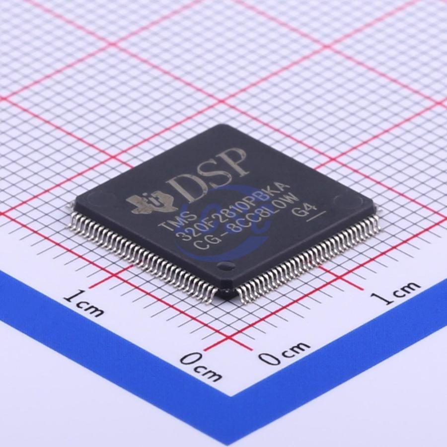
TMS320F2810PBKA TI
TI

TMS320F2810PBKA

150MHz LQFP-128(14x14) Microcontrollers RoHS

LQFP-128(14x14)ROHS3 CompliantActive

Digital Signal Processors

Manufacturer
TI
Manufacturer part #
TMS320F2810PBKA
Store part #
C394732
Package / case
LQFP-128(14x14)
Packaging
Tray
Datasheet (PDF)

Every Order Guarantee

100% Authentic · 30-Day Return or Replacement · policy

187 in stock

#C394732

Stock & price checked 5 days ago

QuantityUnit pricePack price
1+₹2,862.87₹2,862.87
10+₹2,720.45₹27,204.50
30+₹2,474.14₹74,224.20
90+₹2,259.19₹2,03,327.10

1 × ₹2,862.87

₹2,862.87

excl. GST

₹3,378.19 incl. 18% GST

Need volume or a scheduled delivery? Request a quote
  • Dispatch in 15-18 working days
  • GST invoice with every order
  • Standard pack: 90 per tray

TMS320F2810PBKA

₹2,862.87 for 1 + GST

Need this with the rest of your board? Upload the BOM — we price every line.Upload BOM

Specifications

Operating Temperature
-40℃~+85℃
Clock Rate
150MHz

Packaging & compliance

RoHS
ROHS3 Compliant
Lifecycle
Active
ECCN
3A991A2
Packaging
Tray
Standard pack
90 / Tray
Sold per
Piece
Minimum order
1
Unit weight
2.536 g

Overview

The TMS320F2810, TMS320F2811, and TMS320F2812 devices are members of the TMS320C28x DSP family, offering highly integrated, high-performance solutions for demanding control applications.

Applications

  • Advanced Driver Assistance Systems (ADAS)
  • Building Automation
  • Electronic Point of Sale
  • EV/HEV Powertrain
  • Factory Automation
  • Grid Infrastructure
  • Industrial Transportation
  • Medical, Healthcare & Fitness
  • Motor Drivers
  • Power Delivery
  • Telecom Infrastructure
  • Test and Measurement

Key features

  • High-performance static CMOS technology
  • 150MHz (6.67ns cycle time)
  • Low-power design (1.8V core voltage at 135MHz, 1.9V core voltage at 150MHz, 3.3V I/O)
  • JTAG boundary scan support
  • IEEE Standard 1149.1-1990 IEEE Standard Test Access Port and Boundary-Scan Architecture
  • High-performance 32-bit CPU (TMS320C28x)
  • 16×16 and 32×32 MAC operations
  • 16×16 dual MAC
  • Harvard bus architecture
  • Atomic operations
  • Fast interrupt response and processing
  • Unified memory programming model
  • 4M linear program/data address range
  • Efficient code (C/C++ and assembly)
  • TMS320F24x/LF240x processor source-code compatible
  • On-chip memory
  • Up to 128K×16 flash memory (four 8K×16 and six 16K×16 sectors)
  • 1K×16 OTP ROM
  • L0 and L1: two 4K×16 single-cycle access RAM (SARAM) blocks
  • H0: one 8K×16 SARAM block
  • M0 and M1: two 1K×16 SARAM blocks
  • Boot ROM (4K×16)
  • Software boot modes supported
  • Standard math tables
  • External interface (F2812)
  • Total memory greater than 1M×16
  • Programmable wait states
  • Programmable read/write strobe timing
  • Three independent chip selects
  • Byte ordering: little-endian
  • Clock and system control
  • On-chip oscillator
  • Watchdog timer module
  • Three external interrupts
  • Peripheral interrupt expansion (PIE) block supporting 45 peripheral interrupts
  • Three 32-bit CPU timers
  • 128-bit security key/lock
  • Protects flash/OTP and L0/L1 SARAM
  • Prevents firmware reverse engineering
  • Motor control peripherals
  • Two event managers (EVA, EVB)
  • Compatible with 240xA devices
  • Serial port peripherals
  • Serial Peripheral Interface (SPI)
  • Two Serial Communication Interfaces (SCI), standard UART
  • Enhanced Controller Area Network (eCAN)
  • Multi-channel Buffered Serial Port (McBSP)
  • 12-bit ADC, 16 channels
  • 2×8 channel input multiplexer
  • Two sample-and-hold
  • Single/simultaneous conversion
  • Fast conversion rate: 80ns/12.5MSPS
  • Up to 56 general-purpose I/O (GPIO) pins
  • Advanced emulation features
  • Analysis and breakpoint functions
  • Real-time debug via hardware
  • Development tools include
  • ANSI C/C++ compiler/assembler/linker
  • Code Composer Studio/IDE
  • DSP/BIOS
  • JTAG scan controller
  • IEEE Standard 1149.1-1990 IEEE Standard Test Access Port and Boundary-Scan Architecture
  • Low-power modes for power savings
  • Idle, standby, and halt modes supported
  • Individual peripheral clock disable
  • Temperature options
  • A: -40℃ to 85℃ (GHH, ZHH, PGF, PBK)
  • S: -40℃ to 125℃ (GHH, ZHH, PGF, PBK)
  • Q: -40℃ to 125℃ (PGF, PBK) (AEC-Q100 qualified for automotive applications)

Same category

More in Microcontrollers

View all