


STC Micro
STC8H1K08-36I-TSSOP2051 Series 8 Bit 33MHz TSSOP-20 Microcontrollers RoHS
From
₹42.36
1,52,934 in stock
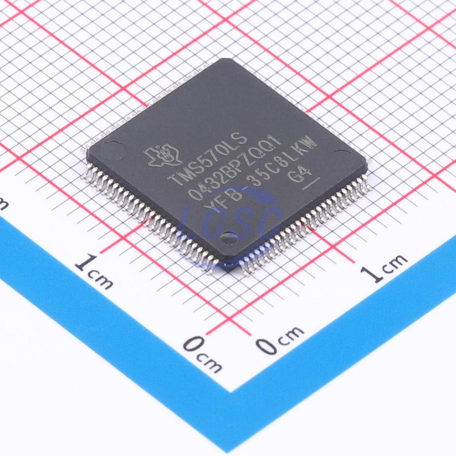
ARM Cortex-R4 16/32 Bit 80MHz QFP-100(14x14) Microcontrollers RoHS
16-bit and 32-bit RISC flash microcontrollers
Every Order Guarantee
100% Authentic · 30-Day Return or Replacement · policy
1,013 in stock
#C2053708
Stock & price checked 2 days ago
| Quantity | Unit price | Pack price |
|---|---|---|
| 1+ | ₹1,413.53 | ₹1,413.53 |
| 10+ | ₹1,260.50 | ₹12,605.00 |
| 30+ | ₹1,162.61 | ₹34,878.30 |
| 100+ | ₹1,068.00 | ₹1,06,800.00 |
1 × ₹1,413.53
₹1,413.53
excl. GST
₹1,667.97 incl. 18% GST
TMS5700432BPZQQ1R
₹1,413.53 for 1 + GST
The TMS570LS0432/0332 devices are high-performance automotive-grade microcontrollers suitable for safety systems. The safety architecture includes two CPUs in lockstep, CPU and memory BIST logic, ECC on flash and data SRAM, parity on peripheral memories, and loopback functionality on peripheral I/Os. The TMS570LS0432/0332 devices integrate an ARM Cortex-R4 CPU. This CPU has an efficient performance of 1.66 DMIPS/MHz and can operate at a frequency of up to 80 MHz, thus providing a computing power of up to 132 DMIPS. This device supports the big-endian (BE32) format. The TMS570LS0432/0332 devices have 384 KB and 256 KB of integrated flash memory respectively, along with 32 KB of data RAM. Both the flash and RAM have single-bit error correction and double-bit error detection capabilities. The flash memory on this device is an electrically erasable and programmable non-volatile memory implemented through a 64-bit wide data bus interface. The flash uses a 3.3V power supply input voltage (the same level as the I/O power supply) for all read, programming, and erase operations. In pipeline mode, the flash operates at a system clock frequency of 80 MHz. The SRAM supports single-cycle read and write access in byte, half-word, word, and double-word modes across the entire supported frequency range. The TMS570LS0432/0332 devices are designed for real-time control applications and include a next-generation high-end timer (N2HET) timing coprocessor (with up to 19 I/O ports) and a 12-bit analog-to-digital converter (ADC) with 16 inputs in a 100-pin package. The N2HET is an advanced intelligent timer that can provide precise timing for real-time applications. This timer is software-controlled, uses a small instruction set, and has a dedicated timer microcomputer and accompanying I/O ports. The N2HET can be used for pulse-width modulation output, capture or compare input, or as a GPIO. The N2HET is particularly suitable for applications that require multiple sensor information with complex and accurate time pulses and drive actuators. A high-end timer transfer unit (HTU) can perform DMA-type processing to transfer N2HET data to and from the main memory. A memory protection unit (MPU) is built into the HTU. The enhanced quadrature encoder pulse (eQEP) module is used for direct connection with linear or rotary incremental encoders to obtain position, direction, and speed information from rotating machines used in high-performance motion and position control systems. This device has a 12-bit resolution MibADC with 16 channels and a 64-word buffer RAM with parity protection. The MibADC channels can be converted independently or grouped by software for sequential conversion sequences. There are three independent groups. Each sequence can be converted once when triggered or configured for continuous conversion mode. This MibADC has a 10-bit mode that can be used when compatibility with earlier devices is required or when a higher conversion rate is needed. This device has multiple communication interfaces: one MibSPI, two SPIs, one UART/LIN, and two UART/LINs. The SPI provides a convenient method for high-speed communication between similar shift register type devices. The UART/LIN supports the Local Interconnect Standard 2.1 and can be used as a full-duplex mode UART using the standard non-return-to-zero (NRZ) format. The DCAN supports the CAN 2.0 (A and B) protocol standards and uses a serial, multi-master communication protocol that effectively supports distributed real-time control with a robust communication rate of up to 1 Mbps. The DCAN is well-suited for applications operating in noisy and harsh environments (such as automotive and industrial applications) that require reliable serial communication or multi-wire cabling. The frequency-modulated phase-locked loop (FMPLL) clock module is used to multiply an external frequency reference by a higher frequency for internal use. The FMPLL can provide one of five possible clock source inputs to the global clock module (GCM). The GCM can manage the mapping between available clock sources and the device clock domains. This device also has an external clock prescaler (ECP) module. When enabled, this circuit outputs a continuous external clock on the ECLK pin. The ECLK frequency is a user-programmable ratio of a peripheral interface clock (VCLK) frequency. This low-frequency output, which can be externally monitored, serves as an indicator of the device's operating frequency. The error signaling module (ESM) can monitor all device errors and determine whether to trigger an interrupt or switch the external nERROR pin when a fault is detected. The nERROR pin can be externally monitored as an indicator of a fault condition within the microcontroller. The I/O multiplexing control module (IOMM) can configure input/output pins to support alternative functions. With integrated safety features and a wide selection of communication and control peripherals, the TMS570LS0432/0332 is an ideal solution for real-time control applications.
Similar parts — check the datasheet before substituting.
| Part | Manufacturer | Package | Stock | Price from (excl. GST) | Action | |
|---|---|---|---|---|---|---|
| TMS5700432BPZQQ1#C1337398TI · QFP-100(14x14) | TI | QFP-100(14x14) | 6 | ₹1,250.80 · 6 in stock | View | |
Same category
STC Micro
STC8H1K08-36I-TSSOP2051 Series 8 Bit 33MHz TSSOP-20 Microcontrollers RoHS
From
₹42.36
1,52,934 in stock
PUYA
PY32F002BF15U6TRARM Cortex-M0+ 32 Bit 24MHz QFN-20-EP(3x3) Microcontrollers
From
₹23.27
82,295 in stock
STC Micro
STC8G1K08A-36I-SOP851 Series 8 Bit 36MHz SOP-8 Microcontrollers RoHS
From
₹35.85
82,120 in stock
SILICON LABS
EFM8BB21F16G-C-QFN20R51 Series 8 Bit 50MHz QFN-20-EP(3x3) Microcontrollers RoHS
From
₹167.39
59,815 in stock




