RENESAS
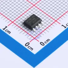
AT25DF021A-MAHNHR-T
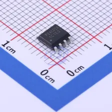
2Mbit 1.7V~3.6V 85MHz SPI UDFN-8(3x2) Memory RoHS
UDFN-8(3x2)ROHS3 CompliantActive
SPI Interface Flash Memory Chip Performance
Datasheet (PDF)
Every Order Guarantee
100% Authentic · 30-Day Return or Replacement · policy
10 in stock
#C21638863
Stock & price checked 38 h ago
| Quantity | Unit price | Pack price |
|---|---|---|
| 1+ | ₹297.36 | ₹297.36 |
| 10+ | ₹290.78 | ₹2,907.80 |
| 30+ | ₹286.26 | ₹8,587.80 |
| 100+ | ₹281.93 | ₹28,193.00 |
1 × ₹297.36
₹297.36
excl. GST
₹350.88 incl. 18% GST
- Dispatch in 15-18 working days
- GST invoice with every order
- Standard pack: 5,000 per reel
AT25DF021A-MAHNHR-T
₹297.36 for 1 + GST
Specifications
- Operating Temperature
- -40℃~+125℃
- Features
- Write enable latch;Hardware write protection;Software write protection
- Memory Size
- 2Mbit
- Voltage - Supply
- 1.7V~3.6V
- Program / Erase Cycles
- 200,000 cycles
- Clock Frequency
- 85MHz
- Data Retention - TDR (Year)
- 20 Years
- Interface
- SPI
Packaging & compliance
- RoHS
- ROHS3 Compliant
- Lifecycle
- Active
- ECCN
- EAR99
- Packaging
- Tape & Reel (TR)
- Standard pack
- 5,000 / Reel
- Sold per
- Piece
- Minimum order
- 1
- Unit weight
- 0.51 g
Overview
Key features
- Single 1.65 V - 3.6 V Supply (-40℃ to +85℃)
- Single 1.7 V - 3.6 V Supply (-40℃ to +125℃)
- Serial Peripheral Interface (SPI) Compatible
- Supports SPI Modes 0 and 3
- Supports Dual I/O Operation
- 104 MHz Maximum Operating Frequency
- Clock-to-Output (tCO) of 6 ns
- Flexible, Optimized Erase Architecture for Code + Data Storage Application
- Small (256 Byte) Page Erase
- Uniform 4-kByte Block Erase
- Uniform 32-kByte Block Erase
- Uniform 64-kByte Block Erase
- Full Chip Erase
- Hardware Controlled Locking of Protected Sectors through WP Pin
- 128-Byte Programmable One-Time Programmable (OTP) Security Register
- 64 Bytes factory programmed with a unique identifier
- 64 Bytes user programmable
- Flexible Programming
- Byte/Page Program (1 to 256 Bytes)
- Dual-Input Byte/Page Program (1 to 256 Bytes)
- Sequential Program Mode Capability
- Fast Program and Erase Times
- 1.25 ms Typical Page Program (256 Bytes) Time
- 40 ms Typical 4-kByte Block Erase Time
- 250 ms Typical 32-kByte Block Erase Time
- 500 ms Typical 64-kByte Block Erase Time
- Automatic Checking and Reporting of Erase/Program Failures
- Software Controlled Reset
- JEDEC Standard Manufacturer and Device ID Read Methodology
- Low Power Dissipation
- 200 nA Ultra Deep Power Down current (Typical)
- 4.5 μA Deep Power-Down Current (Typical)
- 25 μA Standby current (Typical)
- 4.5 mA Active Read Current (Typical)
- Endurance:
- 100,000 Program/Erase Cycles (-40℃ to +85℃)
- 20,000 Program/Erase Cycles (-40℃ to +125℃)
- Data Retention: 20 Years
- Complies with Full Industrial Temperature Range
- Industry Standard Green (Pb/Halide-free/RoHS Compliant) Package Options
- 8-lead SOIC (150-mil)
- 8-pad Ultra Thin DFN (2x3x0.6 mm)
- 8-pad Ultra Thin DFN (5x6x0.6 mm)
- 8-lead TSSOP
- 8-ball WLCSP (3x2x3 ball matrix)
Alternatives
Similar parts — check the datasheet before substituting.
| Part | Manufacturer | Package | Stock | Price from (excl. GST) | Action | |
|---|---|---|---|---|---|---|
 | BY25Q20AWUIG(R)#C50176337BOYAMICRO · USON-8(2x3) | BOYAMICRO | USON-8(2x3) | 2,965 | ₹13.92 · 2,965 in stock | View |
 | AT25DF021A-MAHN-T#C2061529RENESAS · UDFN-8-EP(2x3) | RENESAS | UDFN-8-EP(2x3) | 10 | ₹304.63 · 10 in stock | View |
 | ZD25WD20BUIGR#C2759918Zetta · USON-8-EP(2x3) | Zetta | USON-8-EP(2x3) | 17,285 | ₹14.70 · 17,285 in stock | View |
 | ZD25WD20CEIGR#C7462744Zetta · USON-8(2x3) | Zetta | USON-8(2x3) | 2,750 | ₹17.66 · 2,750 in stock | View |
 | AT25EU0021A-MAHN-T#C6127444RENESAS · UDFN-8(2x3) | RENESAS | UDFN-8(2x3) | 50 | ₹91.17 · 50 in stock | View |
Same category